 ChipApex | Global Electronic Components Supplier

SEARCH
Search Product
Search Post
— IC芯片 | 连接器 | 传感器 | 被动器件 —
Search productSearch post
— IC芯片 | 连接器 | 传感器 | 被动器件 —
Consult the customer manager about the wholesale price.
consultation hotline:86-132-6715-2157
email:[email protected]
Contact the product manager for consultation. One-stop consultation is available.
Do you want a lower wholesale price? Please send us your inquiry and we will reply immediately.
SIT92110AI-N is listed in the Clock Buffers, Drivers range at ChipApex. The manufacturer field lists SiTime. Its product description is -40C TO 85C, 32PIN, 5050, 1.8V-3. Review the specifications below when checking this part for your BOM.
The SiTime SIT92110AI-N is a 10-output low-jitter clock fan-out buffer designed for high-frequency clock and data distribution. It features a 3:1 input multiplexer with primary, secondary, and crystal inputs, distributing the selected signal to ten LVCMOS output drivers. The device supports core supply voltages of 3.3 V, 2.5 V, or 1.8 V, and output supplies of 3.3 V, 2.5 V, 1.8 V, or 1.5 V. It operates within an ambient temperature range of -40°C to +85°C and is housed in a 32-pin, 5 mm x 5 mm QFN package.
Verify the specific ordering suffix against the manufacturer's current datasheet to confirm package type, temperature range, and revision status. Ensure that the required supply voltage levels (VDD and VDDO) match the design specifications, as the device supports multiple independent voltage domains without sequencing requirements.
Select this component when a 10-channel LVCMOS output buffer is required with ultra-low additive jitter. Consider the input signal compatibility, as the universal inputs accept various differential and single-ended formats. Ensure the PCB layout supports the specified slew rate requirements (>2 V/ns) to maintain optimal phase noise and jitter performance.
The SIT92110 belongs to SiTime's family of high-performance clock buffers. It utilizes MEMS technology for timing generation and distribution. The AI suffix typically denotes industrial temperature grade availability, while the N suffix indicates the specific package variant. This part serves as a direct replacement for traditional quartz-based fan-out buffers in demanding applications.
Public confirmed substitute part numbers are not available in the provided documentation. Verify pinout and electrical characteristics carefully when considering alternative vendors or previous revisions of the same part number.
The maximum input frequency is 250 MHz for LVDS, LVPECL, HCSL, and LVCMOS outputs.
Yes, the core supply (VDD) and output supply (VDDO) are independent, allowing for level translation between different voltage domains without requiring supply sequencing.
Pulling the OE pin LOW forces the outputs to a high-impedance state after four falling edges of the input signal. Pulling OE HIGH enables the outputs.
Explore related parts through Clock/Timing, Integrated Circuits (ICs), all product categories, ChipApex homepage.
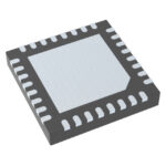 SIT92110AI-N
SIT92110AI-N is listed in the Clock Buffers, Drivers range at ChipApex. The manufacturer field lists SiTime. Its product description is -40C TO 85C, 32PIN,…
Read More
Select MOV varistors by continuous voltage, clamping behavior, surge waveform and repetition. Check thermal disconnection, fuse coordination and replacements.
Read More
SIT92110AI-N is listed in the Clock Buffers, Drivers range at ChipApex. The manufacturer field lists SiTime. Its product description is -40C TO 85C, 32PIN,…
Read More
SIT92110AI-N is listed in the Clock Buffers, Drivers range at ChipApex. The manufacturer field lists SiTime. Its product description is -40C TO 85C, 32PIN,…
Read More
Choose logic inverter ICs by thresholds, supply, output drive and delay. Compare standard and Schmitt-trigger inputs, power sequencing and replacement checks.
Read More
SIT92110AI-N is listed in the Clock Buffers, Drivers range at ChipApex. The manufacturer field lists SiTime. Its product description is -40C TO 85C, 32PIN,…
Read More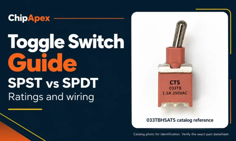
Compare SPST and SPDT toggle switches, understand AC/DC ratings, and follow wiring examples. Check contact action, mounting and parts in the ChipApex catalog.
Read More
SIT92110AI-N is listed in the Clock Buffers, Drivers range at ChipApex. The manufacturer field lists SiTime. Its product description is -40C TO 85C, 32PIN,…
Read More
SIT92110AI-N is listed in the Clock Buffers, Drivers range at ChipApex. The manufacturer field lists SiTime. Its product description is -40C TO 85C, 32PIN,…
Read More
SIT92110AI-N is listed in the Clock Buffers, Drivers range at ChipApex. The manufacturer field lists SiTime. Its product description is -40C TO 85C, 32PIN,…
Read More
SIT92110AI-N is listed in the Clock Buffers, Drivers range at ChipApex. The manufacturer field lists SiTime. Its product description is -40C TO 85C, 32PIN,…
Read More
SIT92110AI-N is listed in the Clock Buffers, Drivers range at ChipApex. The manufacturer field lists SiTime. Its product description is -40C TO 85C, 32PIN,…
Read More
The activity of extra discounts on wholesale prices is in full swing…
Please fill in your contact information and we will send you the latest wholesale price list.






