 ChipApex | Global Electronic Components Supplier

SEARCH
Search Product
Search Post
— IC芯片 | 连接器 | 传感器 | 被动器件 —
Search productSearch post
— IC芯片 | 连接器 | 传感器 | 被动器件 —
Consult the customer manager about the wholesale price.
consultation hotline:86-132-6715-2157
email:[email protected]
Contact the product manager for consultation. One-stop consultation is available.
Do you want a lower wholesale price? Please send us your inquiry and we will reply immediately.
SL18861DI is listed in the Clock Buffers, Drivers range at ChipApex. The manufacturer field lists Skyworks Solutions Inc.. Its product description is IC CLK BUFFER 1:3 52MHZ 10TDFN. Review the specifications below when checking this part for your BOM.
The SL18861DI is a high-performance 3-output clock distribution buffer manufactured by Silicon Laboratories. It provides three single-ended LVCMOS outputs from a single input clock using proprietary low phase noise and low power dissipation circuit design. The device operates on a single power supply ranging from 1.70V to 3.65V, with typical current consumption of 2.7mA at 1.8V. It supports an input clock frequency range of 10MHz to 52MHz for both LVCMOS square wave and sine wave inputs. Each output features individual enable control (OE1/2/3) to reduce power consumption when connected devices are inactive.
Verify package type upon ordering; the standard SL18861DI ships in a tube, while the SL18861DIT variant uses tape and reel packaging. Both options utilize the same 10-pin TDFN package and industrial temperature range (-40°C to 85°C). Confirm RoHS compliance status as per manufacturer specifications.
Select based on required supply voltage within the 1.70V to 3.65V range. Ensure load capacitance requirements do not exceed 20pF (typical) or 25pF (max at 3.3V). Verify that input signal levels match LVCMOS thresholds or sine wave swing requirements for the chosen VDD.
This component belongs to the Silicon Laboratories clock distribution buffer family. It is designed to isolate devices driven by clock outputs to minimize interference between them. The device integrates control logic to manage output states and includes an OE_OSC pin to enable external TCXO/XO oscillators when all outputs are disabled.
No public confirmed substitute part numbers are available in the provided documentation. Evaluate alternatives based on matching 3-channel LVCMOS output configuration, 10-52MHz frequency range, and 10-pin TDFN package dimensions.
Each output has a dedicated enable pin (OE1, OE2, OE3). When the respective OE pin is high, the output is active; when low, the output enters a Hi-Z state.
The OE_OSC pin enables an external TCXO/XO. It goes low only when OE1, OE2, and OE3 are all low; otherwise, it remains high.
The typical load capacitance is 10pF, with a maximum rating of 20pF at 1.8V/2.5V and 25pF at 3.3V.
Explore related parts through Clock/Timing, Integrated Circuits (ICs), all product categories, ChipApex homepage.
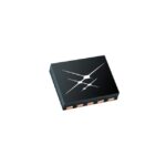 SL18861DI

SL18861DI is listed in the Clock Buffers, Drivers range at ChipApex. The manufacturer field lists Skyworks Solutions Inc.. Its product description is IC CLK…
Read More
SL18861DI is listed in the Clock Buffers, Drivers range at ChipApex. The manufacturer field lists Skyworks Solutions Inc.. Its product description is IC CLK…
Read More
SL18861DI is listed in the Clock Buffers, Drivers range at ChipApex. The manufacturer field lists Skyworks Solutions Inc.. Its product description is IC CLK…
Read More
SL18861DI is listed in the Clock Buffers, Drivers range at ChipApex. The manufacturer field lists Skyworks Solutions Inc.. Its product description is IC CLK…
Read More
SL18861DI is listed in the Clock Buffers, Drivers range at ChipApex. The manufacturer field lists Skyworks Solutions Inc.. Its product description is IC CLK…
Read More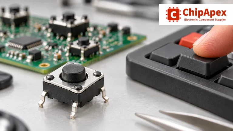
Choose tactile switches by operating force, travel, actuator height, footprint and lifetime. Check debounce, sealing and the assembled button mechanism.
Read More
SL18861DI is listed in the Clock Buffers, Drivers range at ChipApex. The manufacturer field lists Skyworks Solutions Inc.. Its product description is IC CLK…
Read More
SL18861DI is listed in the Clock Buffers, Drivers range at ChipApex. The manufacturer field lists Skyworks Solutions Inc.. Its product description is IC CLK…
Read More
SL18861DI is listed in the Clock Buffers, Drivers range at ChipApex. The manufacturer field lists Skyworks Solutions Inc.. Its product description is IC CLK…
Read More
SL18861DI is listed in the Clock Buffers, Drivers range at ChipApex. The manufacturer field lists Skyworks Solutions Inc.. Its product description is IC CLK…
Read More
SL18861DI is listed in the Clock Buffers, Drivers range at ChipApex. The manufacturer field lists Skyworks Solutions Inc.. Its product description is IC CLK…
Read More
Select MOV varistors by continuous voltage, clamping behavior, surge waveform and repetition. Check thermal disconnection, fuse coordination and replacements.
Read More
The activity of extra discounts on wholesale prices is in full swing…
Please fill in your contact information and we will send you the latest wholesale price list.






