 ChipApex | Global Electronic Components Supplier

SEARCH
Search Product
Search Post
— IC芯片 | 连接器 | 传感器 | 被动器件 —
Search productSearch post
— IC芯片 | 连接器 | 传感器 | 被动器件 —
Consult the customer manager about the wholesale price.
consultation hotline:86-132-6715-2157
email:[email protected]
Contact the product manager for consultation. One-stop consultation is available.
Do you want a lower wholesale price? Please send us your inquiry and we will reply immediately.
SN74ABT126DB is listed in the Buffers, Drivers, Receivers, Transceivers range at ChipApex. The manufacturer field lists Texas Instruments. Its product description is BUS DRIVER, ABT SERIES. Review the specifications below when checking this part for your BOM.
The SN74ABT126DB is a quadruple bus buffer gate with 3-state outputs manufactured by Texas Instruments. It operates within a supply voltage range of 4.5 V to 5.5 V and supports an operating temperature range from -40°C to +85°C. The device features high-drive outputs capable of sourcing -32 mA and sinking 64 mA. Propagation delays are specified at a maximum of 6.3 ns for tPLH and 5.7 ns for tPHL at VCC = 5 V. It includes Ioff support for hot insertion and maintains a high-impedance state during power-up or power-down when VCC is between 0 and 2.1 V.
Verify the specific ordering suffix 'DB' corresponds to the SSOP package type and tape-and-reel quantity as listed in the manufacturer's documentation. Confirm RoHS compliance status and lead finish details via the official Package Option Addendum before finalizing procurement specifications.
Select this component for applications requiring non-inverting quadruple buffering with 3-state control. Ensure the system operates within the 4.5 V to 5.5 V supply voltage range and accommodates the required drive currents. Consider the SSOP package dimensions and thermal impedance characteristics for PCB layout constraints.
This part belongs to the SN74ABT126 family of quadruple bus buffer gates. It shares functional similarities with other ABT series logic devices but is distinguished by its specific pinout, package configuration, and electrical characteristics defined in the SN54ABT126/SN74ABT126 datasheet.
Direct substitutes include SN74ABT126DR (SOIC package) and SN74ABT126NSR (SOP package). Verify package compatibility and pin alignment before substitution.
When VCC is between 0 and 2.1 V, the device enters a high-impedance state. To ensure this state above 2.1 V, OE should be tied to GND through a pulldown resistor.
Latch-up performance exceeds 500 mA per JESD 17 standards.
Explore related parts through Logic, Integrated Circuits (ICs), all product categories, ChipApex homepage.
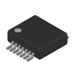 SN74ABT126DB

SN74ABT126DB is listed in the Buffers, Drivers, Receivers, Transceivers range at ChipApex. The manufacturer field lists Texas Instruments. Its product description is BUS DRIVER,…
Read More
SN74ABT126DB is listed in the Buffers, Drivers, Receivers, Transceivers range at ChipApex. The manufacturer field lists Texas Instruments. Its product description is BUS DRIVER,…
Read More
SN74ABT126DB is listed in the Buffers, Drivers, Receivers, Transceivers range at ChipApex. The manufacturer field lists Texas Instruments. Its product description is BUS DRIVER,…
Read More
Learn how a diode conducts, how to identify anode and cathode, and when to choose rectifier, TVS, Zener or photodiode types for a circuit.
Read More
SN74ABT126DB is listed in the Buffers, Drivers, Receivers, Transceivers range at ChipApex. The manufacturer field lists Texas Instruments. Its product description is BUS DRIVER,…
Read More
SN74ABT126DB is listed in the Buffers, Drivers, Receivers, Transceivers range at ChipApex. The manufacturer field lists Texas Instruments. Its product description is BUS DRIVER,…
Read More
SN74ABT126DB is listed in the Buffers, Drivers, Receivers, Transceivers range at ChipApex. The manufacturer field lists Texas Instruments. Its product description is BUS DRIVER,…
Read More
SN74ABT126DB is listed in the Buffers, Drivers, Receivers, Transceivers range at ChipApex. The manufacturer field lists Texas Instruments. Its product description is BUS DRIVER,…
Read More
SN74ABT126DB is listed in the Buffers, Drivers, Receivers, Transceivers range at ChipApex. The manufacturer field lists Texas Instruments. Its product description is BUS DRIVER,…
Read More
SN74ABT126DB is listed in the Buffers, Drivers, Receivers, Transceivers range at ChipApex. The manufacturer field lists Texas Instruments. Its product description is BUS DRIVER,…
Read More
SN74ABT126DB is listed in the Buffers, Drivers, Receivers, Transceivers range at ChipApex. The manufacturer field lists Texas Instruments. Its product description is BUS DRIVER,…
Read More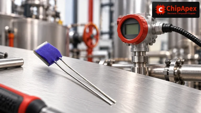
Compare Pt100 and Pt1000 RTDs, two-, three- and four-wire connections, excitation and self-heating. Build an error budget from element to reported temperature.
Read More
The activity of extra discounts on wholesale prices is in full swing…
Please fill in your contact information and we will send you the latest wholesale price list.





