 ChipApex | Global Electronic Components Supplier

SEARCH
Search Product
Search Post
— IC芯片 | 连接器 | 传感器 | 被动器件 —
Search productSearch post
— IC芯片 | 连接器 | 传感器 | 被动器件 —
Consult the customer manager about the wholesale price.
consultation hotline:86-132-6715-2157
email:[email protected]
Contact the product manager for consultation. One-stop consultation is available.
Do you want a lower wholesale price? Please send us your inquiry and we will reply immediately.
SN74LS245DW is listed in the Buffers, Drivers, Receivers, Transceivers range at ChipApex. The manufacturer field lists Texas Instruments. Its product description is IC TXRX NON-INVERT 5.25V 20SOIC. Review the specifications below when checking this part for your BOM.
The SN74LS245DW is an octal bus transceiver utilizing Schottky transistor logic, designed for asynchronous bidirectional communication between data buses. It features three-state outputs and operates within a supply voltage range of 4.75 V to 5.25 V. The device provides a low-level output current of 24 mA and a high-level output current of -15 mA. Typical propagation delay times are 8 ns from port to port, with maximum delays reaching 12 ns under specified load conditions.
Verify the specific package variant against the orderable addendum, as the DW suffix indicates SOIC packaging which may have different availability status compared to other variants like DWR or N. Confirm RoHS compliance and lead finish specifications directly with Texas Instruments documentation prior to finalizing procurement orders.
Select this component for applications requiring standard LS logic compatibility with higher drive strength than basic TTL. Ensure the design accommodates the 0°C to 70°C operating temperature range. Verify that input signal levels meet the specified VIH and VIL thresholds for reliable operation within the recommended supply voltage parameters.
This device belongs to the SNx4LS245 family of octal bus transceivers. It shares common pinouts and functional definitions with related parts such as the SN54LS245 and SN74LS245N, differing primarily in manufacturing grade, package type, and specific electrical characteristics defined by the logic series.
SN74LS245DWR
When the DIR input is Low, data transfers from the B bus to the A bus. When DIR is High, data transfers from the A bus to the B bus.
The Output Enable (OE) input is active-low. When OE is Low, all channels are active. When OE is High, the outputs enter a high-impedance state, effectively isolating the buses.
Explore related parts through Logic, Integrated Circuits (ICs), all product categories, ChipApex homepage.
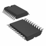 SN74LS245DW

SN74LS245DW is listed in the Buffers, Drivers, Receivers, Transceivers range at ChipApex. The manufacturer field lists Texas Instruments. Its product description is IC TXRX…
Read More
SN74LS245DW is listed in the Buffers, Drivers, Receivers, Transceivers range at ChipApex. The manufacturer field lists Texas Instruments. Its product description is IC TXRX…
Read More
SN74LS245DW is listed in the Buffers, Drivers, Receivers, Transceivers range at ChipApex. The manufacturer field lists Texas Instruments. Its product description is IC TXRX…
Read More
SN74LS245DW is listed in the Buffers, Drivers, Receivers, Transceivers range at ChipApex. The manufacturer field lists Texas Instruments. Its product description is IC TXRX…
Read More
SN74LS245DW is listed in the Buffers, Drivers, Receivers, Transceivers range at ChipApex. The manufacturer field lists Texas Instruments. Its product description is IC TXRX…
Read More
Choose an ADC converter by resolution, sample rate, noise and input design. Review practical tradeoffs and prepare component requirements for ChipApex.
Read More
SN74LS245DW is listed in the Buffers, Drivers, Receivers, Transceivers range at ChipApex. The manufacturer field lists Texas Instruments. Its product description is IC TXRX…
Read More
Understand voltage controlled oscillator tuning, phase noise and PLL operation. Check supply noise, output loading and requirements before selection.
Read More
Understand UART protocol framing, baud rate and electrical interfaces. Learn 8N1 timing, TX/RX wiring, buffering and practical troubleshooting steps.
Read More
SN74LS245DW is listed in the Buffers, Drivers, Receivers, Transceivers range at ChipApex. The manufacturer field lists Texas Instruments. Its product description is IC TXRX…
Read More
SN74LS245DW is listed in the Buffers, Drivers, Receivers, Transceivers range at ChipApex. The manufacturer field lists Texas Instruments. Its product description is IC TXRX…
Read More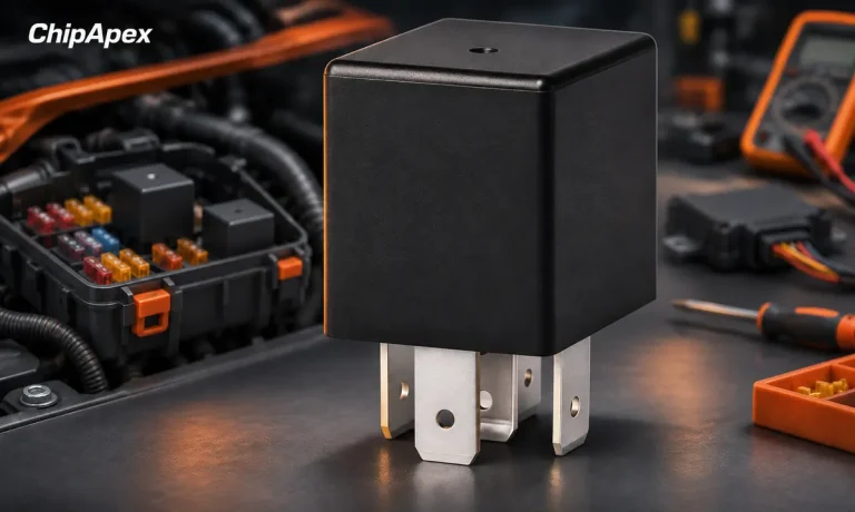
Understand automotive relay terminals, coil suppression and load ratings. Check inrush, socket compatibility and temperature before selecting a replacement.
Read More
The activity of extra discounts on wholesale prices is in full swing…
Please fill in your contact information and we will send you the latest wholesale price list.





