 ChipApex | Global Electronic Components Supplier

SEARCH
Search Product
Search Post
— IC芯片 | 连接器 | 传感器 | 被动器件 —
Search productSearch post
— IC芯片 | 连接器 | 传感器 | 被动器件 —
Consult the customer manager about the wholesale price.
consultation hotline:86-132-6715-2157
email:[email protected]
Contact the product manager for consultation. One-stop consultation is available.
Do you want a lower wholesale price? Please send us your inquiry and we will reply immediately.
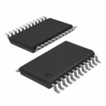
SN74LVC828APWT is listed in the Buffers, Drivers, Receivers, Transceivers range at ChipApex. The manufacturer field lists Texas Instruments. Its product description is IC BUFFER INVERT 3.6V 24TSSOP. Review the specifications below when checking this part for your BOM.
The SN74LVC828APWT is a 10-bit buffer and bus driver with 3-state outputs manufactured by Texas Instruments. It operates from a supply voltage range of 1.65 V to 3.6 V and features inputs that accept voltages up to 5.5 V, supporting mixed-mode signal operation in 5-V input/output environments with a 3.3-V VCC. The device provides an inverting data path at its outputs and utilizes two active-low output-enable (OE1 and OE2) inputs configured as a 2-input AND gate. It supports partial-power-down mode via Ioff circuitry and includes ESD protection exceeding JESD 22 standards.
Verify the package type matches the specific suffix requirements for your assembly process. The APWT suffix indicates a TSSOP package variant supplied in a small tape and reel format. Confirm the operating temperature range aligns with your design specifications before procurement. Ensure all unused inputs are properly terminated to maintain device functionality.
Select this component when designing systems requiring 10-bit data buffering with mixed-voltage compatibility between 3.3-V and 5-V logic levels. The dual active-low output enable inputs provide flexible control over the 3-state outputs. Consider the low static power consumption and high-speed propagation characteristics suitable for general-purpose digital applications within the specified voltage range.
This part belongs to the SN74LVC828A series of 10-bit buffers and drivers with 3-state outputs. It is designed for low-voltage CMOS applications and offers high-performance bus interfacing capabilities. The device is available in multiple package options including SOIC, SSOP, TSSOP, and TVSOP formats to accommodate various PCB layout requirements.
SN74LVC828ADGVR
The device incorporates Ioff circuitry that disables the outputs when powered down, preventing damaging current backflow through the device.
OE1 and OE2 are active-low output-enable inputs that function as a 2-input AND gate; if either input is high, all ten outputs enter the high-impedance state.
Explore related parts through Logic, Integrated Circuits (ICs), all product categories, ChipApex homepage.
 SN74LVC828APWT

SN74LVC828APWT is listed in the Buffers, Drivers, Receivers, Transceivers range at ChipApex. The manufacturer field lists Texas Instruments. Its product description is IC BUFFER…
Read More
SN74LVC828APWT is listed in the Buffers, Drivers, Receivers, Transceivers range at ChipApex. The manufacturer field lists Texas Instruments. Its product description is IC BUFFER…
Read More
SN74LVC828APWT is listed in the Buffers, Drivers, Receivers, Transceivers range at ChipApex. The manufacturer field lists Texas Instruments. Its product description is IC BUFFER…
Read More
SN74LVC828APWT is listed in the Buffers, Drivers, Receivers, Transceivers range at ChipApex. The manufacturer field lists Texas Instruments. Its product description is IC BUFFER…
Read More
SN74LVC828APWT is listed in the Buffers, Drivers, Receivers, Transceivers range at ChipApex. The manufacturer field lists Texas Instruments. Its product description is IC BUFFER…
Read More
SN74LVC828APWT is listed in the Buffers, Drivers, Receivers, Transceivers range at ChipApex. The manufacturer field lists Texas Instruments. Its product description is IC BUFFER…
Read More
SN74LVC828APWT is listed in the Buffers, Drivers, Receivers, Transceivers range at ChipApex. The manufacturer field lists Texas Instruments. Its product description is IC BUFFER…
Read More
SN74LVC828APWT is listed in the Buffers, Drivers, Receivers, Transceivers range at ChipApex. The manufacturer field lists Texas Instruments. Its product description is IC BUFFER…
Read More
SN74LVC828APWT is listed in the Buffers, Drivers, Receivers, Transceivers range at ChipApex. The manufacturer field lists Texas Instruments. Its product description is IC BUFFER…
Read More
SN74LVC828APWT is listed in the Buffers, Drivers, Receivers, Transceivers range at ChipApex. The manufacturer field lists Texas Instruments. Its product description is IC BUFFER…
Read More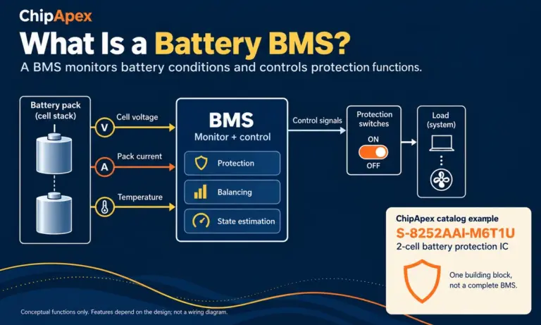
Learn what a battery BMS does, how protection differs from charging, and which pack specifications to check when sourcing BMS components through ChipApex.
Read More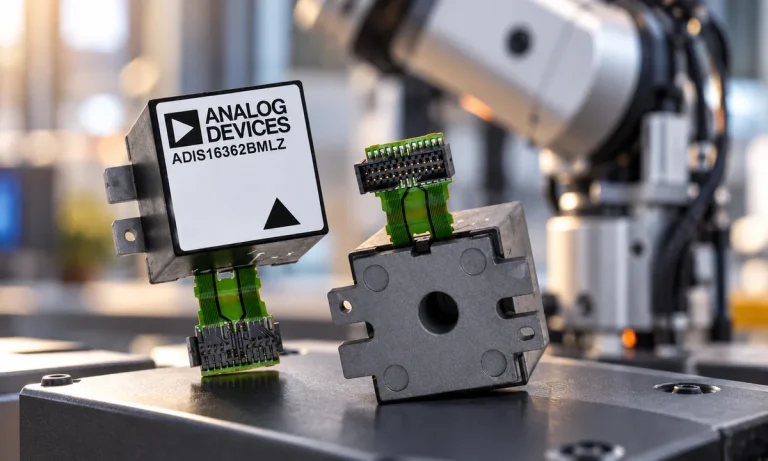
Learn what an IMU measures, how accelerometers and gyroscopes work together, why orientation estimates drift, and what to compare.
Read More
The activity of extra discounts on wholesale prices is in full swing…
Please fill in your contact information and we will send you the latest wholesale price list.





