 ChipApex | Global Electronic Components Supplier

SEARCH
Search Product
Search Post
— IC芯片 | 连接器 | 传感器 | 被动器件 —
Search productSearch post
— IC芯片 | 连接器 | 传感器 | 被动器件 —
Consult the customer manager about the wholesale price.
consultation hotline:86-132-6715-2157
email:[email protected]
Contact the product manager for consultation. One-stop consultation is available.
Do you want a lower wholesale price? Please send us your inquiry and we will reply immediately.
SSR1N60BTM is listed in the Single FETs, MOSFETs range at ChipApex. The manufacturer field lists onsemi. Its product description is MOSFET N-CH 600V 900MA DPAK. Review the specifications below when checking this part for your BOM.
The SSR1N60BTM is a 600V N-Channel enhancement mode power MOSFET manufactured by onsemi, utilizing Fairchild's planar DMOS technology. It features a maximum continuous drain current of 0.9A at 25°C and a typical static drain-source on-resistance of 9.7Ω at VGS = 10V. The device offers a low total gate charge of 5.9nTypical and a reverse transfer capacitance of 3.6pF. It supports a single pulsed avalanche energy of 50mJ and operates within a junction temperature range of -55°C to +150°C.
Verify the specific ordering suffix 'TM' against official documentation to confirm package type and tape-and-reel specifications. Ensure compatibility with D-PAK or I-PAK mechanical footprints as defined in the datasheet. Confirm RoHS compliance status and check for any lifecycle notices regarding obsolescence before finalizing procurement plans.
Select this component for applications requiring robust avalanche ruggedness and low gate charge. Evaluate thermal management requirements based on the specified junction-to-case thermal resistance. Consider the maximum continuous drain current derating curve when designing for elevated case temperatures above 25°C.
This part belongs to the SSR1N60B / SSU1N60B family of 600V N-Channel MOSFETs originally produced by Fairchild Semiconductor. The SSR prefix typically denotes the D-PAK package, while SSU indicates the I-PAK package. These devices are engineered for general-purpose high-voltage switching applications.
Direct substitutes include the SSR1N60B and SSU1N60B variants from the same manufacturer family. Verify pinout compatibility and ensure that replacement parts meet the same electrical ratings for voltage, current, and thermal performance.
The peak diode recovery dv/dt is rated at 5.5 V/ns under specified test conditions.
Yes, the datasheet specifies that the devices are 100% avalanche tested with a single pulsed avalanche energy (EAS) of 50 mJ.
Explore related parts through FETs, MOSFETs, Transistors, Discrete Semiconductor Products, all product categories.
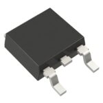 SSR1N60BTM

SSR1N60BTM is listed in the Single FETs, MOSFETs range at ChipApex. The manufacturer field lists onsemi. Its product description is MOSFET N-CH 600V 900MA…
Read More
SSR1N60BTM is listed in the Single FETs, MOSFETs range at ChipApex. The manufacturer field lists onsemi. Its product description is MOSFET N-CH 600V 900MA…
Read More
SSR1N60BTM is listed in the Single FETs, MOSFETs range at ChipApex. The manufacturer field lists onsemi. Its product description is MOSFET N-CH 600V 900MA…
Read More
Learn what data acquisition means, from sensors and conditioning to sampling and storage. Review channel timing, wiring, calibration and data quality.
Read More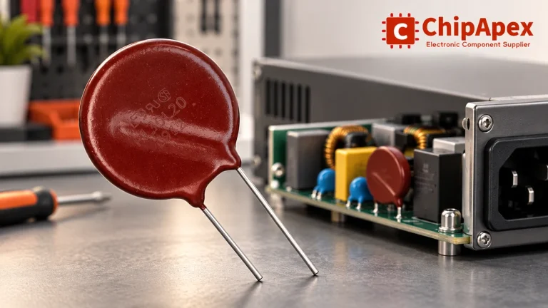
Select MOV varistors by continuous voltage, clamping behavior, surge waveform and repetition. Check thermal disconnection, fuse coordination and replacements.
Read More
SSR1N60BTM is listed in the Single FETs, MOSFETs range at ChipApex. The manufacturer field lists onsemi. Its product description is MOSFET N-CH 600V 900MA…
Read More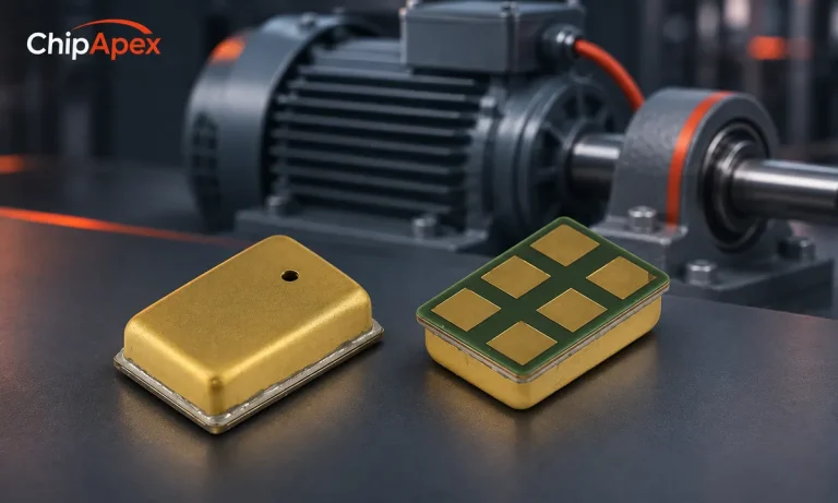
Choose a vibration sensor for machine monitoring. Compare sensing methods, bandwidth, noise and mounting, then define the signal-chain requirements.
Read More
SSR1N60BTM is listed in the Single FETs, MOSFETs range at ChipApex. The manufacturer field lists onsemi. Its product description is MOSFET N-CH 600V 900MA…
Read More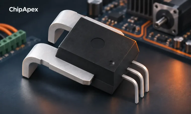
Compare Hall, shunt, current transformer and Rogowski sensing. Check AC/DC capability, accuracy, isolation, heat and response before selecting a sensor.
Read More
SSR1N60BTM is listed in the Single FETs, MOSFETs range at ChipApex. The manufacturer field lists onsemi. Its product description is MOSFET N-CH 600V 900MA…
Read More
SSR1N60BTM is listed in the Single FETs, MOSFETs range at ChipApex. The manufacturer field lists onsemi. Its product description is MOSFET N-CH 600V 900MA…
Read More
SSR1N60BTM is listed in the Single FETs, MOSFETs range at ChipApex. The manufacturer field lists onsemi. Its product description is MOSFET N-CH 600V 900MA…
Read More
The activity of extra discounts on wholesale prices is in full swing…
Please fill in your contact information and we will send you the latest wholesale price list.





