 ChipApex | Global Electronic Components Supplier

SEARCH
Search Product
Search Post
— IC芯片 | 连接器 | 传感器 | 被动器件 —
Search productSearch post
— IC芯片 | 连接器 | 传感器 | 被动器件 —
The trend of science and technology is changing rapidly.
A transistor controls current in a circuit. It can switch a load on and off or amplify changes in an electrical signal, depending on its connections and operating point. A small control signal influences a larger current path; the energy delivered to the load comes from the circuit's power supply.
A relay driver and an audio input stage may both contain transistors, yet they need different behavior. The driver aims for clear on and off states. The amplifier needs a controlled relationship between input and output over its useful signal range.
The device connects a control terminal to a current-carrying path through semiconductor regions. In a bipolar junction transistor, the terminals are base, collector and emitter. In a field-effect transistor, they are gate, drain and source. The relationships between terminal voltages and currents determine the operating point.
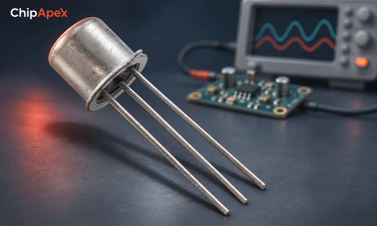
When comparing transistors, identify the circuit role first. Voltage rating, available drive, dissipation and signal frequency all follow from that role. An amplifier's current gain is not a measure of the extra energy the transistor produces; the supply provides that energy while the input controls its delivery.
ROHM's transistor fundamentals and Infineon's operating-principle discussion, listed in the sources, distinguish the two common functions of amplification and switching. Their example circuits also show why the surrounding resistors and supply connections are part of the explanation.
A switch circuit drives the transistor between a low-current off state and a conducting on state. In a low-side arrangement, the device controls the load's connection to the return path. A high-side arrangement controls the connection to the supply and has different drive requirements.
For a bipolar switch, choose base drive using the datasheet's saturation test conditions and the required collector current. A typical small-signal gain value should not be used as a guaranteed saturation design rule. For a MOSFET, check on-resistance at the gate-source voltage the controller can actually supply. Threshold voltage indicates a low-current test point, not full enhancement for a power load.
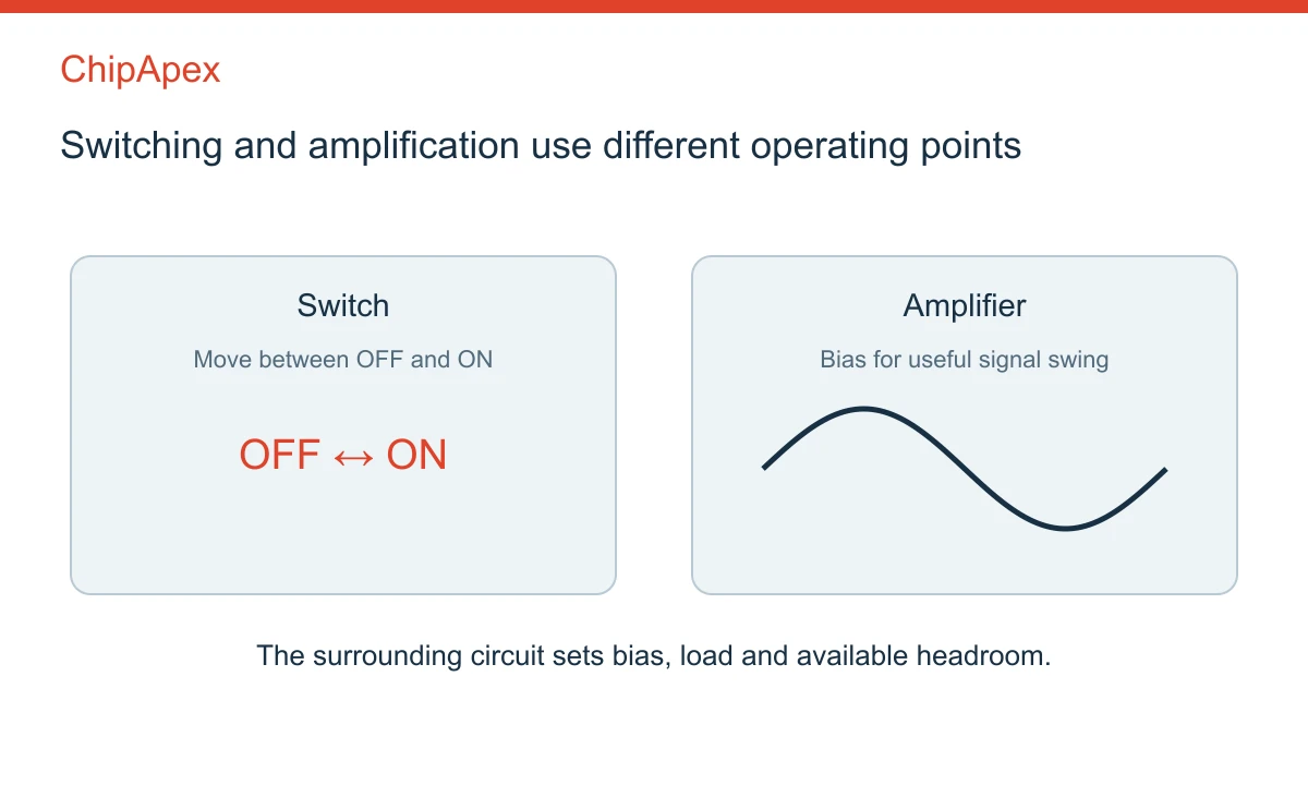
The distinction between operating regions also changes with device type. A BJT used as a low-loss switch commonly operates in saturation. A strongly enhanced MOSFET switch usually operates in its low-resistance region; MOSFET saturation is associated with a different current-voltage relationship. Transferring region names between the devices can cause confusion.
An inductive load such as a relay coil stores energy. When current is interrupted, that energy needs an appropriate path. A flyback diode is one possible solution for a suitable DC coil, while other clamp arrangements can change release time and voltage stress. The suppressor must fit the load and transistor ratings.
An amplifier holds the device at an operating point where input changes produce useful output changes. Bias establishes that starting point. Feedback and the surrounding components can set gain, reduce sensitivity to device variation and control distortion.
If the signal drives the device too far toward cutoff or a voltage limit, the output can clip. Increasing the input then changes the waveform rather than producing a proportional increase in output. Available supply voltage, load, bias current and device limits determine the usable swing.
A small-signal gain specification is measured at stated collector or drain current, voltage and frequency. It does not describe every operating point. Temperature and device spread also matter. Toshiba's discussion of transistor drive explains the relationship between base current and collector current for a BJT, and between gate voltage and channel behavior for a FET.
For a sensor input, evaluate source loading and noise as well as gain. A high source impedance can make leakage and capacitance important. In a complete analog front end, protection, filtering, gain and converter drive must work together; replacing one transistor can change several of those properties.
| Design question | Bipolar transistor | MOSFET |
|---|---|---|
| Control terminals | Base and emitter | Gate and source |
| Drive consideration | Sustained base current in normal conducting operation | Gate-source voltage and charge/discharge current |
| Conducting-state check | Collector-emitter voltage at stated drive conditions | On-resistance at stated gate voltage and temperature |
| Dynamic consideration | Charge storage and switching time | Gate charge, driver impedance and switching transition |
| Common mistake | Using typical gain as a guaranteed switch-drive value | Treating threshold voltage as the required full-load gate drive |
For an illustrative bipolar switch carrying 100 mA, a chosen forced current ratio of 10 would require 10 mA base current. If the assumed control high voltage is 3.3 V and base-emitter drop is 0.8 V, a first resistor estimate is (3.3 − 0.8)/0.01 = 250 Ω. These assumed values explain the method; they are not a validated design. The actual transistor specification and controller output-current limits must support the chosen point.
A MOSFET can draw little steady gate current while still needing substantial current during fast switching. Charging and discharging gate capacitances takes time and energy. A controller that can hold the correct DC voltage may still be too weak to switch a large gate quickly enough for the required frequency.
Absolute maximum ratings are boundaries, not a recommended operating point. A transistor rated for a particular voltage and current cannot necessarily tolerate both simultaneously. Safe operating area, pulse duration and thermal conditions constrain the combination.
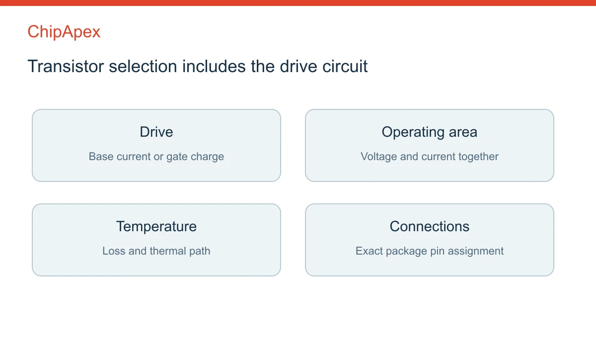
Estimate dissipation at the actual operating point. A BJT conducting 0.5 A with an assumed 0.2 V collector-emitter drop dissipates approximately 0.1 W in that state. Transition losses and other operating states can add to the total. In linear operation, substantial voltage and current can coexist for much longer, changing the thermal and safe-operating-area requirements.
Compare pin assignments from the exact package drawing. Similar metal cans or small surface-mount packages can use different connections. A substitute also needs suitable voltage margin, gain or on-resistance, frequency behavior and thermal performance. Toshiba's datasheet-reading guide explains why several voltage and current ratings appear separately.
The circuit can provide voltage gain, current gain or power gain, depending on its arrangement and loading. Some configurations mainly buffer a signal rather than increasing its voltage. The energy at the output comes from the power supply, and the transistor controls how that energy reaches the load.
Sometimes, with a suitable drive circuit and compatible limits. A bipolar device usually needs a base-current-setting arrangement. A MOSFET needs appropriate gate voltage, controlled startup state and enough drive for its switching charge. Check the microcontroller's pin-current and voltage limits before choosing component values.
Possible causes include insufficient drive, excessive load current, slow transitions or inadequate heat removal. An unsuitable device may spend too much time with both significant voltage and current across it. Measure operating conditions and compare them with the datasheet rather than assuming the package's current rating guarantees cool operation.
They use opposite voltage and current polarities in normal operation, so exchanging them generally requires circuit changes. Pinout and electrical specifications also need review. The same applies when changing between n-channel and p-channel FETs. A similar package does not make the device electrically equivalent.
A transistor controls current electronically, while a mechanical relay moves contacts using a coil. Their drive, isolation, leakage, loss and switching behavior differ. A transistor can drive a relay coil, so both may appear in the same circuit. The appropriate component depends on the required load interface.
For ChipApex, provide the existing part number or the required device type, circuit role, supply, load current, available drive, frequency and package. Include the pinout and thermal constraints for replacements. These details allow a more useful comparison than a nominal current rating alone.
Learn how to use ferrite beads for noise filtering. Check impedance, DC bias, placement, resonance and load-step behavior before selecting a part.
View details
An inductor is approximately linear only over a specified operating range. In the ideal model, its inductance stays constant and voltage equals inductance times the rate of current change. A real magnetic core can approach saturation as current ri...
View details
Understand how motion sensors work. Compare PIR, radar and ultrasonic sensing, then check presence detection, false triggers, optics and signal conditioning.
View details
Learn how a Zener diode regulates voltage. Calculate resistor current and power, check tolerance and temperature, and distinguish Zener and TVS applications.
View details
The activity of extra discounts on wholesale prices is in full swing…
Please fill in your contact information and we will send you the latest wholesale price list.

