 ChipApex | Global Electronic Components Supplier
5SGXMA5N3F45I4G
Search Product
Search Post
— IC芯片 | 连接器 | 传感器 | 被动器件 —
Search productSearch post
— IC芯片 | 连接器 | 传感器 | 被动器件 —
Consult the customer manager about the wholesale price.
consultation hotline:86-132-6715-2157
email:[email protected]
Contact the product manager for consultation. One-stop consultation is available.
Do you want a lower wholesale price? Please send us your inquiry and we will reply immediately.
The Altera 5SGXMA5N3F45I4G is a Stratix V GX Field Programmable Gate Array (FPGA) featuring 840 I/Os and housed in a 1932-BBGA, FCBGA package. It contains 622,000 logic elements, 234,720 Adaptive Logic Modules (ALMs), and 23,472 Logic Array Blocks (LABs). The device includes 50 Mbits of embedded memory and supports data rates up to 14.1 Gb/s with 48 transceivers. Operating voltage ranges from 0.82V to 0.88V, with a junction temperature range of -40°C to 100°C.
Verify the specific suffix codes against official Intel/Altera documentation to ensure correct temperature grade and package variant. Confirm RoHS compliance status and moisture sensitivity level requirements prior to procurement. Check for any recent Product Change Notifications that may affect labeling or specifications.
Compare logic density and transceiver counts against project requirements to ensure optimal resource utilization. Evaluate power consumption profiles at target operating frequencies. Ensure PCB layout capabilities support the 1932-ball BGA package dimensions and thermal dissipation needs.
This component belongs to the Stratix V GX family, designed for high-performance applications requiring significant parallel processing and high-speed serial connectivity. It represents a generation of FPGAs offering substantial logic capacity within a dense ball grid array footprint.
Consult official cross-reference guides for compatible devices within the Stratix V series or newer Agilex families. Verify pin-to-pin compatibility and electrical parameter alignment before substitution.
The integrated transceivers support data rates up to 14.1 Gb/s.
The device contains 23,472 Logic Array Blocks (LABs).
The supply voltage operates between 0.82V and 0.88V.
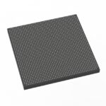 5SGXMA5N3F45I4G
The activity of extra discounts on wholesale prices is in full swing…
Please fill in your contact information and we will send you the latest wholesale price list.





