 ChipApex | Global Electronic Components Supplier
71V2556S100PFGI
Search Product
Search Post
— IC芯片 | 连接器 | 传感器 | 被动器件 —
Search productSearch post
— IC芯片 | 连接器 | 传感器 | 被动器件 —
Consult the customer manager about the wholesale price.
consultation hotline:86-132-6715-2157
email:[email protected]
Contact the product manager for consultation. One-stop consultation is available.
Do you want a lower wholesale price? Please send us your inquiry and we will reply immediately.
The 71V2556S100PFGI is a 4.5 Mbit synchronous static random-access memory (SRAM) integrated circuit manufactured by Renesas Electronics Corporation. It features a parallel interface with a data organization of 128K x 36 bits. The device operates at a maximum clock frequency of 100 MHz and provides an access time of 5 ns. It utilizes a 3.3 V core supply voltage ranging from 3.135 V to 3.465 V and supports 2.5 V I/O levels. The component is housed in a 100-pin Thin Quad Flat Package (TQFP) with dimensions of 14x14 mm. It is designed for surface mount installation and functions within a commercial temperature range of 0°C to +70°C.
Verify the specific suffix PFGI against official Renesas documentation to confirm the 100-pin TQFP package and commercial temperature grade. Confirm RoHS compliance status as it varies by manufacturing date and region. Check for End-of-Life notices, as this part number may be discontinued or subject to production change notifications. Ensure the 2.5V I/O requirement matches the target system's logic levels before procurement.
Select this component when a 36-bit wide data path is required for parallel processing applications. The 100 MHz speed and 5 ns access time suit designs needing moderate-high bandwidth without complex asynchronous timing. Verify that the PCB layout can accommodate the 100-pin TQFP footprint. Consider the 2.5V I/O constraint if interfacing with 3.3V-only logic, necessitating level shifting or compatible drivers.
This device belongs to the 71V2556 family of Zero Bus Turnaround SRAMs. It shares architectural similarities with other variants like the 71V2556S150PFGI but differs in clock speed and access time specifications. The family is characterized by its pipelined synchronous design and 36-bit word width, targeting applications where bus turnaround latency is a critical performance bottleneck.
The 71V2556S133PFGI is a documented similar alternative within the same family, offering higher speed capabilities. Verify pin compatibility and electrical parameter alignment before substitution.
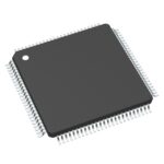 71V2556S100PFGI
The activity of extra discounts on wholesale prices is in full swing…
Please fill in your contact information and we will send you the latest wholesale price list.





