 ChipApex | Global Electronic Components Supplier

SEARCH
Search Product
Search Post
— IC芯片 | 连接器 | 传感器 | 被动器件 —
Search productSearch post
— IC芯片 | 连接器 | 传感器 | 被动器件 —
Consult the customer manager about the wholesale price.
consultation hotline:86-132-6715-2157
email:[email protected]
Contact the product manager for consultation. One-stop consultation is available.
Do you want a lower wholesale price? Please send us your inquiry and we will reply immediately.
74LVC1G19GM,115 is listed in the Signal Switches, Multiplexers, Decoders range at ChipApex. The manufacturer field lists Nexperia USA Inc.. Its product description is IC DECODER/DEMUX 1 X 1:2 6XSON. Review the specifications below when checking this part for your BOM.
The Nexperia 74LVC1G19GM,115 is a single 1-of-2 decoder/demultiplexer housed in an XSON6 package (SOT886). It operates on a supply voltage range of 1.65 V to 5.5 V with inputs tolerant up to 5.5 V. The device features Schmitt-trigger action for noise immunity and includes IOFF circuitry for partial power-down protection. Static characteristics specify low leakage currents and high noise margins across the operating temperature range of -40 °C to +125 °C.
Verify the ordering suffix matches the required package variant. Confirm that the specific revision level aligns with design requirements. Ensure ESD handling procedures are followed due to CMOS sensitivity. Check for any recent product change notifications affecting marking or assembly locations before finalizing procurement.
Select this component for designs requiring a compact 1-of-2 decoding function within tight space constraints. The wide supply voltage compatibility supports mixed-voltage architectures. Verify that the output drive capabilities meet the load requirements of the destination circuitry. Consider the thermal derating characteristics if operating near maximum ambient temperatures.
This device belongs to the 74LVC family of low-voltage CMOS logic components. It provides a specialized decoding function distinct from standard gates or buffers. The XSON6 package offers a minimal footprint suitable for dense PCB layouts. It serves as a fundamental building block for address decoding and data distribution tasks.
NC7SZ19L6X
When the Enable input is HIGH, both outputs 1Y and 2Y assume a HIGH state regardless of the Input A level.
The IOFF circuitry disables the outputs to prevent potentially damaging backflow current through the device when it is powered down.
Explore related parts through Logic, Integrated Circuits (ICs), all product categories, ChipApex homepage.
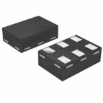 74LVC1G19GM,115

74LVC1G19GM,115 is listed in the Signal Switches, Multiplexers, Decoders range at ChipApex. The manufacturer field lists Nexperia USA Inc.. Its product description is IC…
Read More
74LVC1G19GM,115 is listed in the Signal Switches, Multiplexers, Decoders range at ChipApex. The manufacturer field lists Nexperia USA Inc.. Its product description is IC…
Read More
74LVC1G19GM,115 is listed in the Signal Switches, Multiplexers, Decoders range at ChipApex. The manufacturer field lists Nexperia USA Inc.. Its product description is IC…
Read More
Learn the relay definition, coil and contact operation, NO and NC forms, load ratings and suppression choices. Compare mechanical, reed and solid-state types.
Read More
74LVC1G19GM,115 is listed in the Signal Switches, Multiplexers, Decoders range at ChipApex. The manufacturer field lists Nexperia USA Inc.. Its product description is IC…
Read More
74LVC1G19GM,115 is listed in the Signal Switches, Multiplexers, Decoders range at ChipApex. The manufacturer field lists Nexperia USA Inc.. Its product description is IC…
Read More
Learn how a diode conducts, how to identify anode and cathode, and when to choose rectifier, TVS, Zener or photodiode types for a circuit.
Read More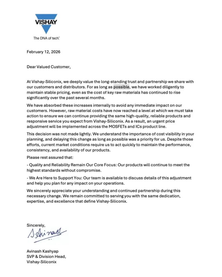
74LVC1G19GM,115 is listed in the Signal Switches, Multiplexers, Decoders range at ChipApex. The manufacturer field lists Nexperia USA Inc.. Its product description is IC…
Read More
74LVC1G19GM,115 is listed in the Signal Switches, Multiplexers, Decoders range at ChipApex. The manufacturer field lists Nexperia USA Inc.. Its product description is IC…
Read More
74LVC1G19GM,115 is listed in the Signal Switches, Multiplexers, Decoders range at ChipApex. The manufacturer field lists Nexperia USA Inc.. Its product description is IC…
Read More
74LVC1G19GM,115 is listed in the Signal Switches, Multiplexers, Decoders range at ChipApex. The manufacturer field lists Nexperia USA Inc.. Its product description is IC…
Read More
74LVC1G19GM,115 is listed in the Signal Switches, Multiplexers, Decoders range at ChipApex. The manufacturer field lists Nexperia USA Inc.. Its product description is IC…
Read More
The activity of extra discounts on wholesale prices is in full swing…
Please fill in your contact information and we will send you the latest wholesale price list.





