 ChipApex | Global Electronic Components Supplier
74LVC2G125DCUTE4
Search Product
Search Post
— IC芯片 | 连接器 | 传感器 | 被动器件 —
Search productSearch post
— IC芯片 | 连接器 | 传感器 | 被动器件 —
Consult the customer manager about the wholesale price.
consultation hotline:86-132-6715-2157
email:[email protected]
Contact the product manager for consultation. One-stop consultation is available.
Do you want a lower wholesale price? Please send us your inquiry and we will reply immediately.
The SN74LVC2G125DCUTE4 is a dual bus buffer gate with 3-state outputs from Texas Instruments. It operates within a supply voltage range of 1.65 V to 5.5 V and supports inputs up to 5.5 V. The device features balanced push-pull CMOS outputs capable of driving ±24 mA at 3.3 V. Propagation delay (tpd) ranges from 1 ns to 9.1 ns depending on voltage and temperature. It includes Ioff circuitry for partial-power-down support and exceeds JESD 22 ESD protection ratings.
Verify the specific package marking and tape-and-reel configuration against the official orderable addendum. Confirm that the DCU package variant matches the required footprint dimensions for PCB layout. Ensure the ordering suffix corresponds to the intended thermal and mechanical specifications provided in the datasheet.
Select this component when designing circuits requiring level translation from 5.5 V logic down to lower supply voltages. It is suitable for applications needing high drive current into light loads or long PCB traces. Consider the NanoFree packaging technology if space constraints are critical, as it utilizes the die as the package structure.
This device belongs to the SN74LVC2G125 family of dual bus buffers. It is part of the broader LVC logic series designed for low-voltage CMOS applications. The family provides standardized functionality for bus holding and direction control across various industrial and consumer electronic systems.
SN74LVC2G125DCTR
The Ioff circuitry forces inputs and outputs into a high-impedance state when the supply voltage is 0 V, preventing damaging current backflow through the device.
Inputs can accept voltages up to 5.5 V, allowing them to be driven above the VCC supply level without damage, provided they remain within absolute maximum ratings.
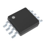 74LVC2G125DCUTE4
The activity of extra discounts on wholesale prices is in full swing…
Please fill in your contact information and we will send you the latest wholesale price list.





