 ChipApex | Global Electronic Components Supplier

SEARCH
Search Product
Search Post
— IC芯片 | 连接器 | 传感器 | 被动器件 —
Search productSearch post
— IC芯片 | 连接器 | 传感器 | 被动器件 —
Consult the customer manager about the wholesale price.
consultation hotline:86-132-6715-2157
email:[email protected]
Contact the product manager for consultation. One-stop consultation is available.
Do you want a lower wholesale price? Please send us your inquiry and we will reply immediately.
9DB403DGILF is listed in the Application Specific Clock/Timing range at ChipApex. The manufacturer field lists Renesas Electronics Corporation. Its product description is IC BUFFER 4OUTPUT DIFF 28TSSOP. Review the specifications below when checking this part for your BOM.
The Renesas Electronics 9DB403DGILF is a zero-delay clock buffer designed for PCI Express (PCIe) applications. It features one HCSL differential input and four HCSL/LVDS differential outputs, supporting frequencies up to 400 MHz. The device operates within a supply voltage range of 3.135 V to 3.465 V and draws 115 mA of operating current. It provides zero propagation delay with a maximum duty cycle distortion of 55%. Packaged in a 28-TSSOP surface-mount enclosure, it functions reliably across an industrial temperature range from -40°C to +85°C.
Verify the suffix 'GILF' corresponds to the TSSOP-28 package and industrial temperature grade (-40°C to +85°C). Confirm RoHS compliance status via the manufacturer datasheet before integration. Ensure the design supports the specified 3.135 V to 3.465 V supply voltage range and 115 mA current consumption requirements.
Select this component when zero-delay skew is critical for PCIe Gen1/Gen2 interfaces. Compare against the 9DB403DGLFT variant if commercial temperature range (0°C to +70°C) suffices for the application environment. Verify that the 28-TSSOP footprint aligns with PCB layout constraints and thermal management capabilities.
This part belongs to the 9DB403 series of PCIe fan-out buffers. It serves as a signal integrity solution for distributing reference clocks in high-speed serial link architectures. The device replaces older buffering solutions by offering integrated HCSL/LVDS output options in a compact surface-mount package.
The 9DB403DGLFT offers identical electrical specifications but operates within a commercial temperature range (0°C to +70°C) instead of the industrial range.
Explore related parts through Clock/Timing, Integrated Circuits (ICs), all product categories, ChipApex homepage.
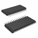 9DB403DGILF

9DB403DGILF is listed in the Application Specific Clock/Timing range at ChipApex. The manufacturer field lists Renesas Electronics Corporation. Its product description is IC BUFFER…
Read More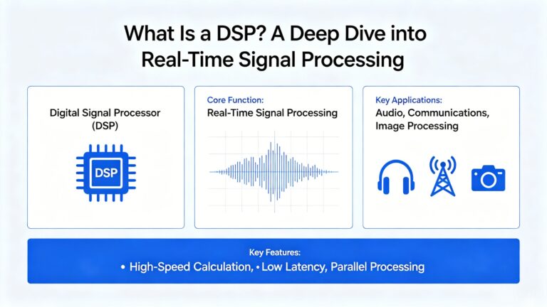
9DB403DGILF is listed in the Application Specific Clock/Timing range at ChipApex. The manufacturer field lists Renesas Electronics Corporation. Its product description is IC BUFFER…
Read More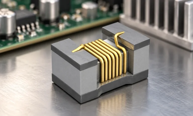
See when an inductor behaves linearly, how DC bias and saturation reduce inductance, and which current and temperature curves to check.
Read More
9DB403DGILF is listed in the Application Specific Clock/Timing range at ChipApex. The manufacturer field lists Renesas Electronics Corporation. Its product description is IC BUFFER…
Read More
9DB403DGILF is listed in the Application Specific Clock/Timing range at ChipApex. The manufacturer field lists Renesas Electronics Corporation. Its product description is IC BUFFER…
Read More
9DB403DGILF is listed in the Application Specific Clock/Timing range at ChipApex. The manufacturer field lists Renesas Electronics Corporation. Its product description is IC BUFFER…
Read More
9DB403DGILF is listed in the Application Specific Clock/Timing range at ChipApex. The manufacturer field lists Renesas Electronics Corporation. Its product description is IC BUFFER…
Read More
9DB403DGILF is listed in the Application Specific Clock/Timing range at ChipApex. The manufacturer field lists Renesas Electronics Corporation. Its product description is IC BUFFER…
Read More
9DB403DGILF is listed in the Application Specific Clock/Timing range at ChipApex. The manufacturer field lists Renesas Electronics Corporation. Its product description is IC BUFFER…
Read More
9DB403DGILF is listed in the Application Specific Clock/Timing range at ChipApex. The manufacturer field lists Renesas Electronics Corporation. Its product description is IC BUFFER…
Read More
9DB403DGILF is listed in the Application Specific Clock/Timing range at ChipApex. The manufacturer field lists Renesas Electronics Corporation. Its product description is IC BUFFER…
Read More9DB403DGILF is listed in the Application Specific Clock/Timing range at ChipApex. The manufacturer field lists Renesas Electronics Corporation. Its product description is IC BUFFER…
Read More
The activity of extra discounts on wholesale prices is in full swing…
Please fill in your contact information and we will send you the latest wholesale price list.






