 ChipApex | Global Electronic Components Supplier
9DBU0441AKLF
Search Product
Search Post
— IC芯片 | 连接器 | 传感器 | 被动器件 —
Search productSearch post
— IC芯片 | 连接器 | 传感器 | 被动器件 —
Consult the customer manager about the wholesale price.
consultation hotline:86-132-6715-2157
email:[email protected]
Contact the product manager for consultation. One-stop consultation is available.
Do you want a lower wholesale price? Please send us your inquiry and we will reply immediately.
The Renesas 9DBU0441AKLF is a 4-output, 1.5V PCIe Zero-Delay/Fanout Clock Buffer designed for low-power applications. It features integrated output terminations providing ZO=100 ohms for direct connection to transmission lines, eliminating external resistors. The device supports LP-HCSL differential signaling with an output frequency range of 1 MHz to 167 MHz. It consumes approximately 45 mW in PLL mode and accepts spread spectrum input for EMI reduction. The component operates at a fixed 1.5V supply voltage and is housed in a space-saving 32-pin VFQFPN package (5.0 x 5.0 mm).
Verify the specific suffix 'KLF' against the manufacturer's current datasheet to confirm pinout and packaging details, as suffixes can indicate variations in tape-and-reel quantity or lead finish. Confirm RoHS compliance status directly with the supplier documentation. Check for End-of-Life (EOL) notices or Last-Time-Buy dates, as clock buffer components may have limited remaining production runs.
Select this component when a 1.5V supply is required for PCIe clocking. Ensure the design utilizes 100Ω differential transmission lines to leverage the integrated termination. Verify that the maximum output frequency requirement does not exceed 167 MHz. Consider the 32-pin VFQFPN footprint constraints during PCB layout. Compare against the 9DMV0441 series if higher voltage (3.3V) or multiplexer functionality is needed instead.
The 9DBU0441 belongs to Renesas' ultra-low-power (ULP) PCIe family of clock buffers. It is part of the broader 9DBU0441 series, which includes variants with different packaging or termination options. This specific model focuses on zero-delay buffering with integrated impedance matching, distinguishing it from standard fanout buffers that require external termination resistors.
The 9DBU0441BKLF is listed as a manufacturer-recommended alternative within the same series. Verify electrical compatibility and pinout equivalence before substitution. Other members of the 9DBU0441 family may offer different package sizes or termination values (e.g., 85Ω), requiring schematic adjustments.
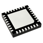 9DBU0441AKLF
The activity of extra discounts on wholesale prices is in full swing…
Please fill in your contact information and we will send you the latest wholesale price list.






