ChipApex | Global Electronic Components Supplier
9DBU0741AKLFT
Search Product
Search Post
— IC芯片 | 连接器 | 传感器 | 被动器件 —
Search productSearch post
— IC芯片 | 连接器 | 传感器 | 被动器件 —
Consult the customer manager about the wholesale price.
consultation hotline:86-132-6715-2157
email:[email protected]
Contact the product manager for consultation. One-stop consultation is available.
Do you want a lower wholesale price? Please send us your inquiry and we will reply immediately.
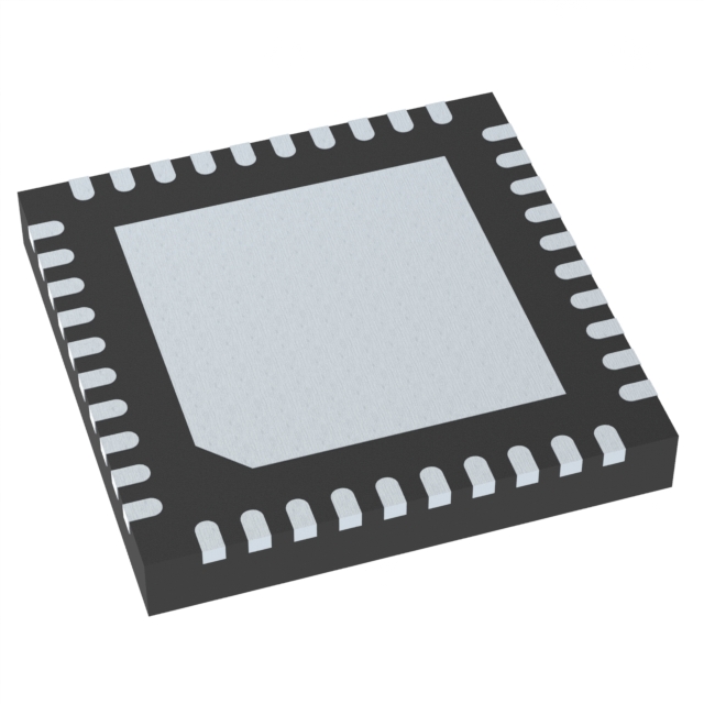
The 9DBU0741AKLFT is a 7-output, 1.5V PCIe fanout clock buffer from Renesas Electronics. It operates within a frequency range of 1 MHz to 167 MHz and supports PCI Express Gen1, Gen2, and Gen3 standards. The device features HCSL differential inputs and LP-HCSL outputs, powered by a 1.425V to 1.575V supply. Packaged in a space-saving 5x5 mm 40-pin VFQFPN with an exposed pad, it includes integrated terminations for direct connection to 100Ω transmission lines. The component functions within a commercial temperature range of 0°C to 70°C.
Verify the package marking and date code against the manufacturer's latest Product Change Notifications (PCNs) prior to procurement. Confirm that the specific suffix matches the required RoHS compliance status. Ensure storage conditions adhere to the Moisture Sensitivity Level (MSL) 3 rating to prevent damage during soldering processes.
Select this component when a seven-channel fanout solution is required for 1.5V PCIe applications. Compare against the 9DBU0941 for nine outputs or the 9DBU0441 for four outputs if channel counts differ. Verify that the input source provides compatible HCSL signals and that the board layout accommodates the 40-pin VFQFPN footprint.
This part belongs to the IDT 1.5V Ultra-Low-Power (ULP) PCIe family, now managed by Renesas Electronics following their acquisition of IDT's timing products. The series is designed to minimize power consumption while maintaining signal integrity for high-speed serial interfaces.
Publicly confirmed substitute part numbers are not available in the provided documentation. Engineering change notices should be reviewed for potential obsolescence or assembly site changes affecting this specific model.
 9DBU0741AKLFT
The activity of extra discounts on wholesale prices is in full swing…
Please fill in your contact information and we will send you the latest wholesale price list.