ChipApex | Global Electronic Components Supplier

SEARCH
Search Product
Search Post
— IC芯片 | 连接器 | 传感器 | 被动器件 —
Search productSearch post
— IC芯片 | 连接器 | 传感器 | 被动器件 —
Consult the customer manager about the wholesale price.
consultation hotline:86-132-6715-2157
email:[email protected]
Contact the product manager for consultation. One-stop consultation is available.
Do you want a lower wholesale price? Please send us your inquiry and we will reply immediately.
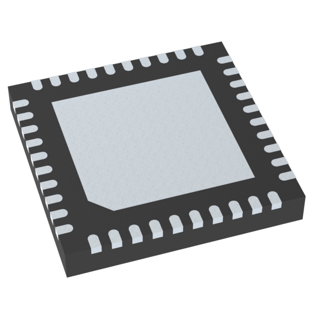
9DBV0741AKLFT is listed in the Application Specific Clock/Timing range at ChipApex. The manufacturer field lists Renesas Electronics Corporation. Its product description is VFQFPN 5.00X5.00X0.90 MM, 0.40MM. Review the specifications below when checking this part for your BOM.
The 9DBV0741AKLFT is a 7-output, 1.8V PCIe fanout clock buffer from Renesas Electronics. It features integrated terminations for direct connection to 100Ω transmission lines, eliminating the need for external resistors. The device supports HCSL differential input and LP-HCSL output signaling with an operating frequency range of 1 MHz to 200 MHz. It includes seven individual output enable pins for power management and three selectable SMBus addresses for configuration. The component is housed in a space-saving 5x5 mm, 32-pin VFQFPN package.
Verify the specific suffix 'AKLFT' against the manufacturer's current datasheet to confirm package type, temperature range, and lead-free status. Note that Renesas timing products are transitioning to SiTime; ensure documentation sources are updated for the latest specifications and availability details.
Select this component when a 1.8V supply is required for PCIe clock distribution. Compare against the 9DBU0741 series if a 1.5V supply or different termination characteristics are needed. Ensure the 200 MHz maximum frequency meets the system's PCIe generation requirements.
This part belongs to the 9DBV05x1-9DBV07x1-9DBV09x1 family of PCIe fanout buffers. These devices are designed to replace standard HCSL buffers by integrating terminations, thereby saving board space and reducing component count. The 9DBV0741 specifically provides seven outputs, bridging the gap between the 5-output and 9-output variants.
The 9DBU0741AKILFT is a similar 7-output buffer but operates at 1.5V instead of 1.8V. Verify voltage compatibility before substitution. Other family members include the 9DBV0541 (5 outputs) and 9DBV0941 (9 outputs).
Explore related parts through Clock/Timing, Integrated Circuits (ICs), all product categories, ChipApex homepage.
 9DBV0741AKLFT
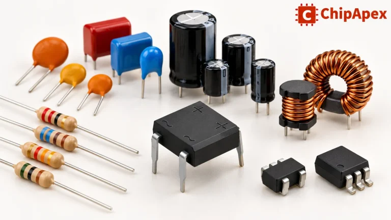
Explore electronic component types, functions, packages and datasheets. Learn selection, replacement and BOM checks before ordering parts for your PCB.
Read More
9DBV0741AKLFT is listed in the Application Specific Clock/Timing range at ChipApex. The manufacturer field lists Renesas Electronics Corporation. Its product description is VFQFPN 5.00X5.00X0.90…
Read More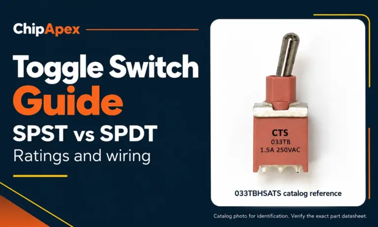
Compare SPST and SPDT toggle switches, understand AC/DC ratings, and follow wiring examples. Check contact action, mounting and parts in the ChipApex catalog.
Read More
9DBV0741AKLFT is listed in the Application Specific Clock/Timing range at ChipApex. The manufacturer field lists Renesas Electronics Corporation. Its product description is VFQFPN 5.00X5.00X0.90…
Read More
9DBV0741AKLFT is listed in the Application Specific Clock/Timing range at ChipApex. The manufacturer field lists Renesas Electronics Corporation. Its product description is VFQFPN 5.00X5.00X0.90…
Read More
Learn the relay definition, coil and contact operation, NO and NC forms, load ratings and suppression choices. Compare mechanical, reed and solid-state types.
Read More
9DBV0741AKLFT is listed in the Application Specific Clock/Timing range at ChipApex. The manufacturer field lists Renesas Electronics Corporation. Its product description is VFQFPN 5.00X5.00X0.90…
Read More
9DBV0741AKLFT is listed in the Application Specific Clock/Timing range at ChipApex. The manufacturer field lists Renesas Electronics Corporation. Its product description is VFQFPN 5.00X5.00X0.90…
Read More
9DBV0741AKLFT is listed in the Application Specific Clock/Timing range at ChipApex. The manufacturer field lists Renesas Electronics Corporation. Its product description is VFQFPN 5.00X5.00X0.90…
Read More
9DBV0741AKLFT is listed in the Application Specific Clock/Timing range at ChipApex. The manufacturer field lists Renesas Electronics Corporation. Its product description is VFQFPN 5.00X5.00X0.90…
Read More
9DBV0741AKLFT is listed in the Application Specific Clock/Timing range at ChipApex. The manufacturer field lists Renesas Electronics Corporation. Its product description is VFQFPN 5.00X5.00X0.90…
Read More
9DBV0741AKLFT is listed in the Application Specific Clock/Timing range at ChipApex. The manufacturer field lists Renesas Electronics Corporation. Its product description is VFQFPN 5.00X5.00X0.90…
Read More
The activity of extra discounts on wholesale prices is in full swing…
Please fill in your contact information and we will send you the latest wholesale price list.