 ChipApex | Global Electronic Components Supplier
9DBV0831AKLF
Search Product
Search Post
— IC芯片 | 连接器 | 传感器 | 被动器件 —
Search productSearch post
— IC芯片 | 连接器 | 传感器 | 被动器件 —
Consult the customer manager about the wholesale price.
consultation hotline:86-132-6715-2157
email:[email protected]
Contact the product manager for consultation. One-stop consultation is available.
Do you want a lower wholesale price? Please send us your inquiry and we will reply immediately.
The 9DBV0831AKLF is an 8-output very low power clock buffer manufactured by Renesas Electronics. Designed for high-speed serial applications, it supports PCIe Gen1 through Gen5 standards with a differential output frequency range of 30 MHz to 137.5 MHz. The device utilizes LP-HCSL output signaling and accepts HCSL differential inputs, including spread spectrum input capabilities. It operates on a single 1..8 V supply voltage with typical power consumption of 62 mW. The component is housed in a space-saving 48-lead VFQFPN package (6.0 x 6.0 mm) and functions within an industrial temperature range of 0°C to +70°C.
Verify the specific suffix 'AKLF' against the manufacturer's current datasheet to confirm pinout, packaging dimensions, and RoHS compliance status. Check for Product Change Notifications (PCNs) regarding assembly site changes or material updates before finalizing procurement plans.
Select this component when designing for PCIe Gen5 or high-speed Ethernet environments requiring low jitter buffering. Ensure the design accommodates the 1.8 V supply rail and utilizes the SMBus interface for dynamic clock management if required. Verify that the 48-VFQFPN package fits the PCB footprint constraints.
This part belongs to the 9DBV0831 family of zero-delay/fanout clock buffers. It serves as a distribution solution for high-frequency clocks in complex digital systems, replacing older generation buffers with lower power profiles and support for newer PCIe specifications.
Publicly confirmed direct substitutes are not listed in the provided documentation. Evaluate other members of the 9DBV series or 9ZXL series only if they match the 1.8 V supply, 8-output configuration, and LP-HCSL signaling requirements.
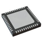 9DBV0831AKLF
The activity of extra discounts on wholesale prices is in full swing…
Please fill in your contact information and we will send you the latest wholesale price list.






