 ChipApex | Global Electronic Components Supplier
AD7870CQ
Search Product
Search Post
— IC芯片 | 连接器 | 传感器 | 被动器件 —
Search productSearch post
— IC芯片 | 连接器 | 传感器 | 被动器件 —
Consult the customer manager about the wholesale price.
consultation hotline:86-132-6715-2157
email:[email protected]
Contact the product manager for consultation. One-stop consultation is available.
Do you want a lower wholesale price? Please send us your inquiry and we will reply immediately.
The AD7870CQ is a complete monolithic 12-bit analog-to-digital converter featuring a 2 μs track-and-hold amplifier and an 8 μs successive approximation ADC. It operates from ±5 V power supplies with a typical power dissipation of 60 mW. The device accepts a bipolar input voltage range of ±3 V and includes an on-chip 3 V buried Zener reference. Dynamic performance specifications include a signal-to-noise ratio of 70 dB at a 10 kHz input frequency and a data access time of 57 ns. The component supports parallel, byte, and serial digital interfaces and is available in a 24-pin dual-in-line package.
Verify the specific suffix C against the manufacturer's current ordering guide to confirm the industrial temperature range and package variant. Ensure the selected version matches the required operating conditions for the target application environment.
Select this model when a ±3 V input range is required. Compare dynamic performance metrics such as SNR and THD against system noise requirements. Verify that the 24-pin DIP package fits the board layout constraints compared to PLCC or SOIC alternatives.
This component belongs to the AD7870/AD7875/AD7876 family of 12-bit sampling ADCs. While sharing the same core architecture and interface logic, variants differ primarily in analog input voltage ranges and package options. The AD7870 specifically targets bipolar ±3 V applications within this series.
The AD7870JNZ and AD7870KPZ are confirmed substitutes within the same product family. Verify pinout compatibility and temperature range specifications before implementation.
The internal laser-trimmed clock is enabled by tying the CLK pin to VSS. An external TTL-compatible clock can be applied to this pin to override the internal oscillator if required.
The REF OUT pin provides the factory-trimmed 3 V internal buried Zener reference voltage. It can supply up to 500 μA to an external load or be used to generate higher reference voltages via scaling circuits.
When held high, the pin selects 12-bit parallel data format. When low or at −5 V, it enables byte or serial data formats, with the latter providing continuous serial clocking at −5 V.
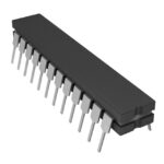 AD7870CQ
The activity of extra discounts on wholesale prices is in full swing…
Please fill in your contact information and we will send you the latest wholesale price list.





