 ChipApex | Global Electronic Components Supplier
AD7892BN-1
Search Product
Search Post
— IC芯片 | 连接器 | 传感器 | 被动器件 —
Search productSearch post
— IC芯片 | 连接器 | 传感器 | 被动器件 —
Consult the customer manager about the wholesale price.
consultation hotline:86-132-6715-2157
email:[email protected]
Contact the product manager for consultation. One-stop consultation is available.
Do you want a lower wholesale price? Please send us your inquiry and we will reply immediately.
The AD7892BN-1 is a high-speed, low-power 12-bit analog-to-digital converter (ADC) fabricated in Analog Devices' LC2MOS process. It operates from a single +5 V supply and features an on-chip track/hold amplifier and a +2.5 V internal reference. This specific model supports ±5 V or ±10 V analog input ranges with a throughput rate of 500 kSPS. It offers both parallel and serial interface options for microprocessor connectivity. The device provides overvoltage protection on analog inputs up to ±17 V and includes a standby mode for power reduction.
Verify the exact ordering suffix to confirm the package type and temperature range specifications. Ensure the selected variant matches the required analog input range configuration for your specific application design constraints.
Select this component when a 12-bit resolution and 500 kSPS sampling rate are required for bipolar input signals. Consider the integrated reference and track/hold amplifier if minimizing external component count is a priority for the system design.
This part belongs to the AD7892 family of single-supply ADCs. Variants within the series differ primarily by their analog input voltage ranges and maximum throughput rates, allowing designers to choose the optimal speed and range combination for their specific signal conditioning needs.
Direct functional substitutes within the same family include the AD7892AN-1 for plastic DIP packaging or the AD7892BR-1 for surface mount SOIC packaging, provided the accuracy and interface requirements remain consistent.
The input range is determined by the connection of the VIN2 pin. Connecting VIN2 to AGND sets the range to ±10 V, while connecting VIN2 to VIN1 sets the range to ±5 V.
The MODE pin selects the data output interface format. A logic high enables the parallel interface mode, while a logic low enables the serial interface mode.
Yes, the internal +2.5 V reference is available at the REF OUT/REF IN pin. However, it should be buffered externally if driving loads other than the ADC itself due to its source impedance.
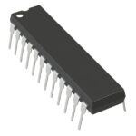 AD7892BN-1
The activity of extra discounts on wholesale prices is in full swing…
Please fill in your contact information and we will send you the latest wholesale price list.





