 ChipApex | Global Electronic Components Supplier

SEARCH
Search Product
Search Post
— IC芯片 | 连接器 | 传感器 | 被动器件 —
Search productSearch post
— IC芯片 | 连接器 | 传感器 | 被动器件 —
Consult the customer manager about the wholesale price.
consultation hotline:86-132-6715-2157
email:[email protected]
Contact the product manager for consultation. One-stop consultation is available.
Do you want a lower wholesale price? Please send us your inquiry and we will reply immediately.
AD9629BCPZRL7-80 is listed in the Analog To Digital Converters (ADC) range at ChipApex. The manufacturer field lists Analog Devices Inc.. Its product description is IC ADC 12BIT PIPELINED 32LFCSP. Review the specifications below when checking this part for your BOM.
The AD9629BCPZRL7-80 is a monolithic, single-channel 12-bit analog-to-digital converter (ADC) from Analog Devices Inc. It operates at a maximum sampling rate of 80 MSPS with a differential input bandwidth of 700 MHz. The device utilizes a multistage differential pipeline architecture with output error correction logic to ensure no missing codes across the full operating temperature range. It requires a single 1.8 V analog supply and supports digital driver supplies ranging from 1.8 V to 3.3 V. Key performance metrics include a Signal-to-Noise Ratio (SNR) of 71.3 dBFS at a 9.7 MHz input frequency and a Spurious-Free Dynamic Range (SFDR) of 95 dBc under the same conditions. Power consumption is rated at 85 mW at the maximum sampling rate.
Verify the specific ordering suffix RL7 indicates reel packaging when sourcing components. Confirm that the BC prefix corresponds to the industrial temperature range specifications (-40°C to +85°C). Ensure compatibility with the 32-lead LFCSP package dimensions during PCB layout. Cross-reference the datasheet revision B for any updates to thermal characteristics or absolute maximum ratings prior to final procurement.
Select this component for applications requiring high linearity and low power consumption at sampling rates up to 80 MSPS. The separate DRVDD supply allows flexibility in interfacing with various logic families. Consider the 8-cycle pipeline latency when designing timing-critical systems. Verify that the input signal amplitude remains within the 2 V p-p differential range to maintain optimal SNR and SFDR performance.
The AD9629 belongs to a family of 12-bit ADCs available in multiple speed grades, including 20 MSPS, 40 MSPS, and 65 MSPS variants. It shares pin compatibility with the AD9609 (10-bit) and AD9649 (14-bit) converters, facilitating migration paths between different resolution requirements while maintaining the same form factor and interface standards.
Direct replacements within the same series include the AD9629BCPZ-20, AD9629BCPZ-40, and AD9629BCPZ-65, which offer lower sampling rates but share identical pinouts and functional interfaces. For higher resolution needs, the AD9649 series serves as a compatible upgrade path.
The AD9629 supports offset binary, gray code, and twos complement data formats, which can be selected via the SPI interface or static control pins.
The ADC accepts differential clock inputs compatible with CMOS, LVDS, or LVP ECL logic levels and includes an internal integer divider allowing for divide-by-1, 2, or 4 ratios.
The exposed paddle serves as the only ground connection for the chip and must be soldered to the analog ground plane to ensure proper functionality, maximize heat dissipation, and improve mechanical strength.
Explore related parts through Data Acquisition, Integrated Circuits (ICs), all product categories, ChipApex homepage.
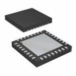 AD9629BCPZRL7-80
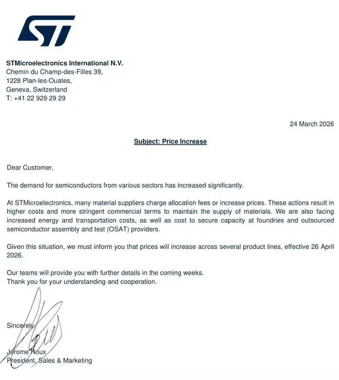
AD9629BCPZRL7-80 is listed in the Analog To Digital Converters (ADC) range at ChipApex. The manufacturer field lists Analog Devices Inc.. Its product description is…
Read More
AD9629BCPZRL7-80 is listed in the Analog To Digital Converters (ADC) range at ChipApex. The manufacturer field lists Analog Devices Inc.. Its product description is…
Read More
Compare RC, crystal and MEMS oscillator circuits. Check ppm, jitter, load capacitance, startup margin and output compatibility before choosing a clock source.
Read More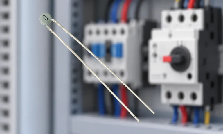
Learn why PTC resistance rises with temperature, how it differs from NTC, and which ratings matter for sensing and protection.
Read More
AD9629BCPZRL7-80 is listed in the Analog To Digital Converters (ADC) range at ChipApex. The manufacturer field lists Analog Devices Inc.. Its product description is…
Read More
AD9629BCPZRL7-80 is listed in the Analog To Digital Converters (ADC) range at ChipApex. The manufacturer field lists Analog Devices Inc.. Its product description is…
Read More
AD9629BCPZRL7-80 is listed in the Analog To Digital Converters (ADC) range at ChipApex. The manufacturer field lists Analog Devices Inc.. Its product description is…
Read More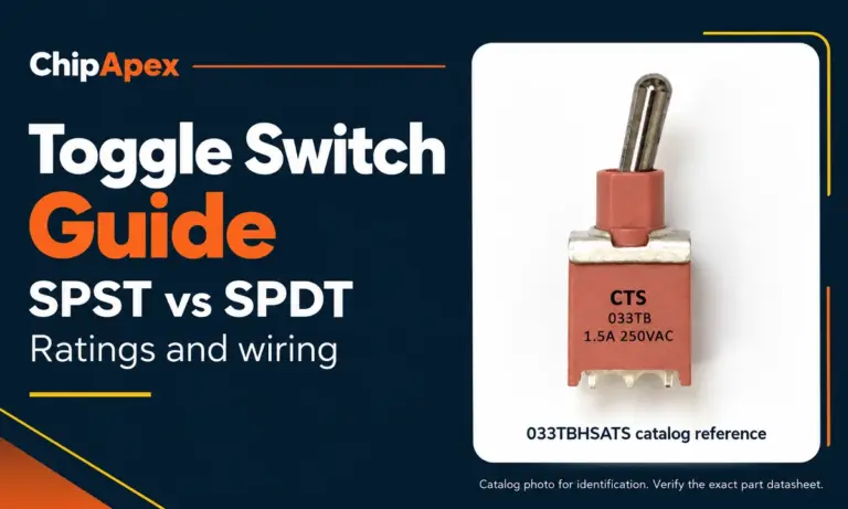
Compare SPST and SPDT toggle switches, understand AC/DC ratings, and follow wiring examples. Check contact action, mounting and parts in the ChipApex catalog.
Read More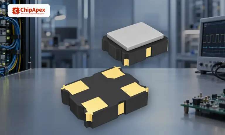
Understand how oscillators generate timing signals, how they differ from crystals, and which frequency, output and stability specs matter when choosing one.
Read More
AD9629BCPZRL7-80 is listed in the Analog To Digital Converters (ADC) range at ChipApex. The manufacturer field lists Analog Devices Inc.. Its product description is…
Read More
AD9629BCPZRL7-80 is listed in the Analog To Digital Converters (ADC) range at ChipApex. The manufacturer field lists Analog Devices Inc.. Its product description is…
Read More
AD9629BCPZRL7-80 is listed in the Analog To Digital Converters (ADC) range at ChipApex. The manufacturer field lists Analog Devices Inc.. Its product description is…
Read More
The activity of extra discounts on wholesale prices is in full swing…
Please fill in your contact information and we will send you the latest wholesale price list.





