 ChipApex | Global Electronic Components Supplier
ADN2818ACPZ-RL7
Search Product
Search Post
— IC芯片 | 连接器 | 传感器 | 被动器件 —
Search productSearch post
— IC芯片 | 连接器 | 传感器 | 被动器件 —
Consult the customer manager about the wholesale price.
consultation hotline:86-132-6715-2157
email:[email protected]
Contact the product manager for consultation. One-stop consultation is available.
Do you want a lower wholesale price? Please send us your inquiry and we will reply immediately.
The ADN2818ACPZ-RL7 is a continuous rate clock and data recovery IC from Analog Devices, designed for serial data inputs ranging from 10 Mbps to 2.7 Gbps. It operates on a single 3 V to 3.6 V supply with a typical current consumption of 180 mA. The device features a proprietary dual-loop architecture that automatically locks to input data rates without an external reference clock. It provides differential CML recovered clock and data outputs in a 5 mm × 5 mm 32-lead LFCSP package.
Verify the specific ADN2818 variant against the ADN2817, as the latter includes additional features like adjustable slice levels and lower power consumption. Confirm package integrity for the 32-LFCSP form factor. Ensure compatibility with the required output voltage standards (CML/LVCMOS/LVDS/LVPECL/LVTTL) supported by the device family.
Select this component when automatic frequency acquisition without a reference clock is required. The ADN2818 is suitable for systems needing integrated limiting amplification. Consider the ADN2817 if higher sensitivity (5 mV p-p) or programmable LOS detection is necessary. Verify thermal management requirements given the 600 mW power dissipation in the compact LFCSP package.
This part belongs to the ADN2817/ADN2818 series of clock and data recovery ICs. It shares the same core architecture and pinout with the ADN2817 but differs in input sensitivity and feature set. The ADN2818 is optimized for applications where moderate input sensitivity is sufficient, offering a balance between performance and power consumption.
Public confirmed substitute part numbers are not available in the provided documentation. The ADN2817 is a related variant within the same family but has distinct electrical characteristics regarding sensitivity and control features.
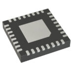 ADN2818ACPZ-RL7
The activity of extra discounts on wholesale prices is in full swing…
Please fill in your contact information and we will send you the latest wholesale price list.







