 ChipApex | Global Electronic Components Supplier

SEARCH
Search Product
Search Post
— IC芯片 | 连接器 | 传感器 | 被动器件 —
Search productSearch post
— IC芯片 | 连接器 | 传感器 | 被动器件 —
Consult the customer manager about the wholesale price.
consultation hotline:86-132-6715-2157
email:[email protected]
Contact the product manager for consultation. One-stop consultation is available.
Do you want a lower wholesale price? Please send us your inquiry and we will reply immediately.
ADN2913ACPZ-RL7 is listed in the Application Specific Clock/Timing range at ChipApex. The manufacturer field lists Analog Devices Inc.. Its product description is IC CLK/DATA REC 8.5GBPS 24-LFCSP. Review the specifications below when checking this part for your BOM.
The ADN2913ACPZ-RL7 is a continuous-rate clock and data recovery IC from Analog Devices, designed for serial data inputs ranging from 6.5 Mbps to 8.5 Gbps. It operates without an external reference clock in standard mode, automatically locking to input data rates. The device features integrated limiting amplifier and equalizer options, with quantizer sensitivity of 6.3 mV typical in limiting amplifier mode. Power supplies include VCC at 1.14 V to 1.26 V, VDD at 2.97 V to 3.63 V, and VCC1 at 1.62 V to 3.63 V. It is housed in a 24-lead LFCSP package.
Verify the specific ordering suffix RL7 against official documentation to confirm reel packaging details. Confirm current availability status as product lifecycle information may indicate end-of-life or limited supply conditions. Ensure compliance with humidity sensitivity levels and soldering guidelines for the LFCSP package during procurement planning.
Select this component for applications requiring CDR functionality up to 8.5 Gbps where no external reference clock is available. Consider power dissipation requirements, which range from 340 mW to 446.6 mW depending on mode and data rate. Verify that the 24-LFCSP package size fits the design constraints and that thermal management meets the specified junction-to-ambient resistance.
The ADN2913 belongs to Analog Devices' family of clock and data recovery ICs. It provides receiver functions including quantization, signal level detection, and clock/data recovery. The device is suitable for high-speed serial communication systems requiring robust jitter performance and flexible input configurations.
Publicly confirmed substitute part numbers are not available in the provided source material. Consult Analog Devices for potential obsolescence notices or alternative recommendations if this part is discontinued.
No, the ADN2913 automatically locks to all data rates without the need for an external reference clock or programming in its standard Lock to Data (LTD) mode.
The typical quantizer sensitivity is 6.3 mV p-p when operating in limiting amplifier mode.
The receiver front-end includes an LOS detector circuit that indicates when the input signal level falls below a user-programmable threshold via I2C. The circuit has hysteresis to prevent chatter at the LOS output.
Explore related parts through Clock/Timing, Integrated Circuits (ICs), all product categories, ChipApex homepage.
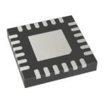 ADN2913ACPZ-RL7
ADN2913ACPZ-RL7 is listed in the Application Specific Clock/Timing range at ChipApex. The manufacturer field lists Analog Devices Inc.. Its product description is IC CLK/DATA…
Read More
ADN2913ACPZ-RL7 is listed in the Application Specific Clock/Timing range at ChipApex. The manufacturer field lists Analog Devices Inc.. Its product description is IC CLK/DATA…
Read More
ADN2913ACPZ-RL7 is listed in the Application Specific Clock/Timing range at ChipApex. The manufacturer field lists Analog Devices Inc.. Its product description is IC CLK/DATA…
Read More
ADN2913ACPZ-RL7 is listed in the Application Specific Clock/Timing range at ChipApex. The manufacturer field lists Analog Devices Inc.. Its product description is IC CLK/DATA…
Read More
ADN2913ACPZ-RL7 is listed in the Application Specific Clock/Timing range at ChipApex. The manufacturer field lists Analog Devices Inc.. Its product description is IC CLK/DATA…
Read More
ADN2913ACPZ-RL7 is listed in the Application Specific Clock/Timing range at ChipApex. The manufacturer field lists Analog Devices Inc.. Its product description is IC CLK/DATA…
Read More
Understand RF attenuator dB values, fixed and programmable types, impedance, power limits and noise tradeoffs before choosing parts for an RF signal path.
Read More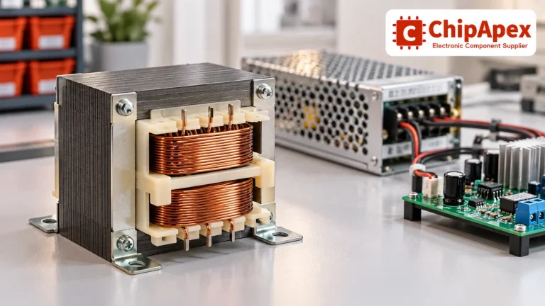
Select power transformers by input frequency, secondary VA, rectifier load, isolation, regulation and inrush. Build a clearer specification for your next RFQ.
Read More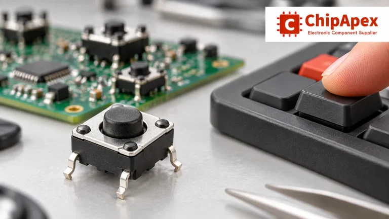
Understand tactile switches, PCB and keyboard differences, four-pin wiring, debounce, force, travel and replacement checks for reliable control inputs.
Read More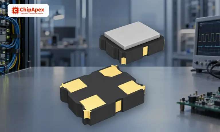
Understand how oscillators generate timing signals, how they differ from crystals, and which frequency, output and stability specs matter when choosing one.
Read More
ADN2913ACPZ-RL7 is listed in the Application Specific Clock/Timing range at ChipApex. The manufacturer field lists Analog Devices Inc.. Its product description is IC CLK/DATA…
Read More
ADN2913ACPZ-RL7 is listed in the Application Specific Clock/Timing range at ChipApex. The manufacturer field lists Analog Devices Inc.. Its product description is IC CLK/DATA…
Read More
The activity of extra discounts on wholesale prices is in full swing…
Please fill in your contact information and we will send you the latest wholesale price list.






