 ChipApex | Global Electronic Components Supplier

SEARCH
Search Product
Search Post
— IC芯片 | 连接器 | 传感器 | 被动器件 —
Search productSearch post
— IC芯片 | 连接器 | 传感器 | 被动器件 —
Consult the customer manager about the wholesale price.
consultation hotline:86-132-6715-2157
email:[email protected]
Contact the product manager for consultation. One-stop consultation is available.
Do you want a lower wholesale price? Please send us your inquiry and we will reply immediately.
AT49F001ANT-55VI is listed in the Memory IC range at ChipApex. The manufacturer field lists Microchip Technology. Its product description is IC FLASH 1MBIT PARALLEL 32VSOP. Review the specifications below when checking this part for your BOM.
The AT49F001ANT-55VI is a 1-megabit (128K x 8) 5-volt only in-system reprogrammable Flash memory manufactured by Microchip Technology. It features a maximum access time of 55 ns and operates within an industrial temperature range of -40°C to +85°C. The device utilizes a sector architecture comprising one 16K-byte boot block, two 8K-byte parameter blocks, and two main memory blocks. It supports byte-by-byte programming with typical times of 30 µs per byte and offers hardware data protection alongside software command sequences for erase and program operations.
Verify the specific suffix VI corresponds to the VSOP package type and 55 ns speed grade as defined in the official ordering information. Confirm the manufacturer origin, noting historical Atmel branding may appear on legacy documentation. Ensure the component meets the specified industrial temperature range requirements for your application environment.
Select this component when a 5-volt only Flash memory solution is required for systems needing in-system reprogrammability. The AT49F001ANT variant provides a compact VSOP package suitable for space-constrained designs. Consider the boot block lockout feature if secure code execution is necessary before main memory updates.
This part belongs to the AT49F001A series of 1-megabit Flash memories. The 'ANT' designation indicates the TSOP or VSOP plastic thin small outline package configuration, while '55' specifies the 55 nanosecond access time performance tier. The 'VI' suffix typically denotes the specific package variant and operating temperature range within the product line.
Compatible substitutes include AT49F001AN-55VI and AT49F001AT-55VI, which share identical electrical specifications but differ in package style. Cross-referencing pinouts and command sequences is recommended when transitioning between package types.
The lockout feature is enabled via a six-step software command sequence involving specific address and data patterns written to the device.
If the boot block programming lockout is enabled, the chip erase function will erase all sectors except the boot block.
Yes, by applying a 12V signal to the RESET pin, the lockout can be overridden to allow erasure or programming of the protected boot block.
Explore related parts through Memory, Integrated Circuits (ICs), all product categories, ChipApex homepage.
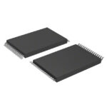 AT49F001ANT-55VI

AT49F001ANT-55VI is listed in the Memory IC range at ChipApex. The manufacturer field lists Microchip Technology. Its product description is IC FLASH 1MBIT PARALLEL…
Read More
AT49F001ANT-55VI is listed in the Memory IC range at ChipApex. The manufacturer field lists Microchip Technology. Its product description is IC FLASH 1MBIT PARALLEL…
Read More
AT49F001ANT-55VI is listed in the Memory IC range at ChipApex. The manufacturer field lists Microchip Technology. Its product description is IC FLASH 1MBIT PARALLEL…
Read More
AT49F001ANT-55VI is listed in the Memory IC range at ChipApex. The manufacturer field lists Microchip Technology. Its product description is IC FLASH 1MBIT PARALLEL…
Read More
Learn how rectifiers convert AC to DC, compare half-wave and bridge circuits, and select voltage, current, recovery and thermal ratings for your design.
Read More
AT49F001ANT-55VI is listed in the Memory IC range at ChipApex. The manufacturer field lists Microchip Technology. Its product description is IC FLASH 1MBIT PARALLEL…
Read More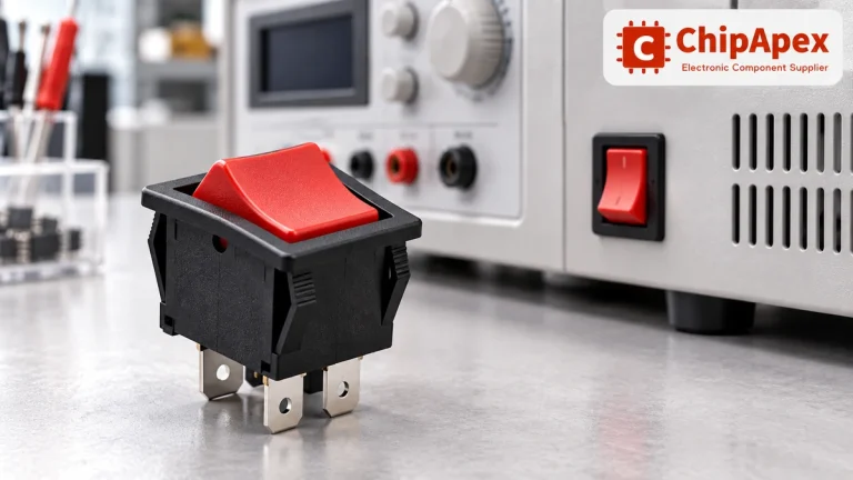
Choose a rocker switch by AC/DC ratings, contact arrangement, illumination, panel fit and sealing. Get practical checks for engineering and component sourcing.
Read More
AT49F001ANT-55VI is listed in the Memory IC range at ChipApex. The manufacturer field lists Microchip Technology. Its product description is IC FLASH 1MBIT PARALLEL…
Read More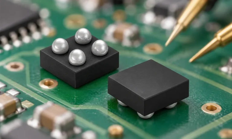
Understand how a comparator switches at a voltage threshold, why hysteresis prevents chatter, and which output and input specs matter.
Read More
AT49F001ANT-55VI is listed in the Memory IC range at ChipApex. The manufacturer field lists Microchip Technology. Its product description is IC FLASH 1MBIT PARALLEL…
Read More
AT49F001ANT-55VI is listed in the Memory IC range at ChipApex. The manufacturer field lists Microchip Technology. Its product description is IC FLASH 1MBIT PARALLEL…
Read More
AT49F001ANT-55VI is listed in the Memory IC range at ChipApex. The manufacturer field lists Microchip Technology. Its product description is IC FLASH 1MBIT PARALLEL…
Read More
The activity of extra discounts on wholesale prices is in full swing…
Please fill in your contact information and we will send you the latest wholesale price list.






