 ChipApex | Global Electronic Components Supplier

SEARCH
Search Product
Search Post
— IC芯片 | 连接器 | 传感器 | 被动器件 —
Search productSearch post
— IC芯片 | 连接器 | 传感器 | 被动器件 —
Consult the customer manager about the wholesale price.
consultation hotline:86-132-6715-2157
email:[email protected]
Contact the product manager for consultation. One-stop consultation is available.
Do you want a lower wholesale price? Please send us your inquiry and we will reply immediately.
CBT3125PW,118 is listed in the Signal Switches, Multiplexers, Decoders range at ChipApex. The manufacturer field lists Nexperia USA Inc.. Its product description is NEXPERIA CBT3125PW - BUS DRIVER,. Review the specifications below when checking this part for your BOM.
The Nexperia CBT3125PW,118 is a quadruple FET bus switch housed in a TSSOP14 package (SOT402-1). It operates within a supply voltage range of 4.5 V to 5.5 V and supports an ambient temperature range from -40 °C to +85 °C. The device features four independent line switches with TTL-compatible input levels. Key electrical characteristics include a typical on-resistance of 5 Ω at 4.5 V and propagation delay of 0.25 ns. It provides robust ESD protection exceeding 2000 V (HBM) and latch-up performance exceeding 500 mA per JESD78.
Verify the specific ordering suffix matches the required package type and tape/reel configuration. Confirm that the component meets RoHS compliance requirements for your manufacturing process. Ensure design reviews account for the specified operating temperature range and absolute maximum ratings to prevent device stress during operation.
Select this component when designing circuits requiring multiple independent bidirectional switches with fast switching speeds. The TTL-compatible inputs simplify interface logic without additional level shifting. Consider the TSSOP14 package dimensions for PCB layout constraints and thermal management requirements relative to the expected current load.
This part belongs to the CBT3125 family of quadruple FET bus switches manufactured by Nexperia. It serves as a solution for managing data flow in digital systems where signal integrity and speed are critical. The PW suffix indicates the TSSOP14 plastic thin shrink small outline package variant.
Direct replacements must match the quadruple FET bus switch functionality and TSSOP14 package. Verify pinout compatibility and electrical parameters such as on-resistance and propagation delay before substitution.
Each switch is disabled when its associated output enable (nOE) input is HIGH. A LOW signal on nOE activates the ON-state, allowing data transfer between ports.
The recommended operating condition specifies a maximum supply voltage (VCC) of 5.5 V. The absolute maximum rating allows up to 7.0 V.
Explore related parts through Logic, Integrated Circuits (ICs), all product categories, ChipApex homepage.
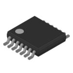 CBT3125PW,118

CBT3125PW,118 is listed in the Signal Switches, Multiplexers, Decoders range at ChipApex. The manufacturer field lists Nexperia USA Inc.. Its product description is NEXPERIA…
Read More
CBT3125PW,118 is listed in the Signal Switches, Multiplexers, Decoders range at ChipApex. The manufacturer field lists Nexperia USA Inc.. Its product description is NEXPERIA…
Read More
CBT3125PW,118 is listed in the Signal Switches, Multiplexers, Decoders range at ChipApex. The manufacturer field lists Nexperia USA Inc.. Its product description is NEXPERIA…
Read More
CBT3125PW,118 is listed in the Signal Switches, Multiplexers, Decoders range at ChipApex. The manufacturer field lists Nexperia USA Inc.. Its product description is NEXPERIA…
Read More
CBT3125PW,118 is listed in the Signal Switches, Multiplexers, Decoders range at ChipApex. The manufacturer field lists Nexperia USA Inc.. Its product description is NEXPERIA…
Read More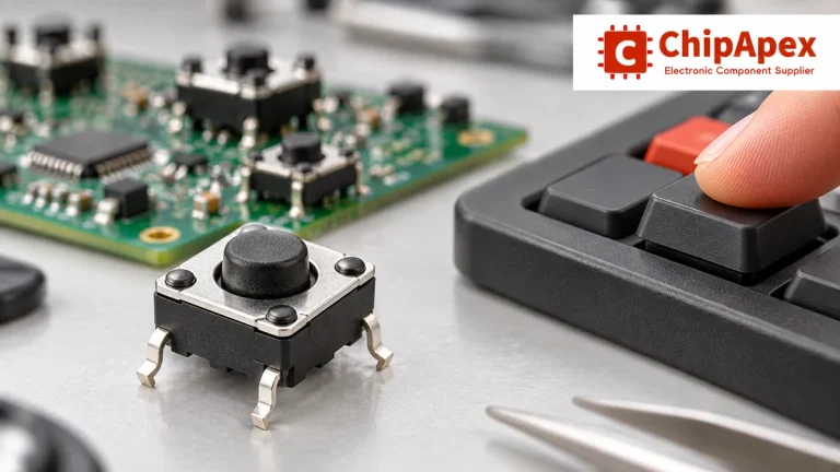
Choose tactile switches by operating force, travel, actuator height, footprint and lifetime. Check debounce, sealing and the assembled button mechanism.
Read More
CBT3125PW,118 is listed in the Signal Switches, Multiplexers, Decoders range at ChipApex. The manufacturer field lists Nexperia USA Inc.. Its product description is NEXPERIA…
Read More
CBT3125PW,118 is listed in the Signal Switches, Multiplexers, Decoders range at ChipApex. The manufacturer field lists Nexperia USA Inc.. Its product description is NEXPERIA…
Read More
CBT3125PW,118 is listed in the Signal Switches, Multiplexers, Decoders range at ChipApex. The manufacturer field lists Nexperia USA Inc.. Its product description is NEXPERIA…
Read More
CBT3125PW,118 is listed in the Signal Switches, Multiplexers, Decoders range at ChipApex. The manufacturer field lists Nexperia USA Inc.. Its product description is NEXPERIA…
Read More
Learn what an integrated circuit is, how ICs work, the main types and the specs to check before choosing a part for your design…
Read More
CBT3125PW,118 is listed in the Signal Switches, Multiplexers, Decoders range at ChipApex. The manufacturer field lists Nexperia USA Inc.. Its product description is NEXPERIA…
Read More
The activity of extra discounts on wholesale prices is in full swing…
Please fill in your contact information and we will send you the latest wholesale price list.





