 ChipApex | Global Electronic Components Supplier

SEARCH
Search Product
Search Post
— IC芯片 | 连接器 | 传感器 | 被动器件 —
Search productSearch post
— IC芯片 | 连接器 | 传感器 | 被动器件 —
Consult the customer manager about the wholesale price.
consultation hotline:86-132-6715-2157
email:[email protected]
Contact the product manager for consultation. One-stop consultation is available.
Do you want a lower wholesale price? Please send us your inquiry and we will reply immediately.
CD4081BCN is listed in the Inverter Gates range at ChipApex. The manufacturer field lists onsemi. Its product description is IC GATE AND 4CH 2-INP 14MDIP. Review the specifications below when checking this part for your BOM.
The CD4081BCN is a monolithic CMOS integrated circuit containing four independent 2-input AND gates. It operates within a DC supply voltage range of 3V to 15V and supports an operating temperature range from -55°C to +125°C. The device features buffered outputs with symmetrical source and sink current capabilities, conforming to standard B series output drive specifications. It provides low power TTL compatibility, allowing a fan-out of two driving 74L logic or one driving 74LS logic. Input protection against static discharge is included via diodes connected to VDD and VSS.
Verify the ordering code matches CD4081BCN to ensure the correct 14-Lead Plastic Dual-In-Line Package (PDIP). Confirm that the required suffix 'X' is omitted if tape and reel packaging is not needed. Ensure the component meets the specified JEDEC MS-001 package dimensions for your board layout requirements.
Select this component when four independent 2-input AND gates are required in a single package. It is suitable for designs needing operation across a wide temperature range and compatibility with both 74L and 74LS logic families. Consider the PDIP-14 package constraints for through-hole mounting versus surface mount alternatives like the BCM variant.
This device belongs to the Quad 2-Input AND Buffered B Series Gate family. It is manufactured by Fairchild Semiconductor Corporation and conforms to standard B series output drive specifications. The part is distinct from the CD4071BC, which provides OR gate functionality instead of AND gates.
CD4081BCM: Same logical function but in SOIC-14 package.
The maximum input leakage current is 1 µA at 15V over the full temperature range.
While not explicitly detailed in the provided text, standard practice for CMOS devices with input protection diodes suggests connecting unused inputs to VDD, VSS, or another input to prevent damage.
Explore related parts through Logic, Integrated Circuits (ICs), all product categories, ChipApex homepage.
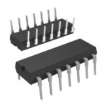 CD4081BCN

CD4081BCN is listed in the Inverter Gates range at ChipApex. The manufacturer field lists onsemi. Its product description is IC GATE AND 4CH 2-INP…
Read More
CD4081BCN is listed in the Inverter Gates range at ChipApex. The manufacturer field lists onsemi. Its product description is IC GATE AND 4CH 2-INP…
Read More
CD4081BCN is listed in the Inverter Gates range at ChipApex. The manufacturer field lists onsemi. Its product description is IC GATE AND 4CH 2-INP…
Read More
Learn how a pressure transducer converts pressure into voltage, current, or digital output, and compare pressure references and key selection specs.
Read More
Select MOV varistors by continuous voltage, clamping behavior, surge waveform and repetition. Check thermal disconnection, fuse coordination and replacements.
Read More
CD4081BCN is listed in the Inverter Gates range at ChipApex. The manufacturer field lists onsemi. Its product description is IC GATE AND 4CH 2-INP…
Read More
CD4081BCN is listed in the Inverter Gates range at ChipApex. The manufacturer field lists onsemi. Its product description is IC GATE AND 4CH 2-INP…
Read More
CD4081BCN is listed in the Inverter Gates range at ChipApex. The manufacturer field lists onsemi. Its product description is IC GATE AND 4CH 2-INP…
Read More
CD4081BCN is listed in the Inverter Gates range at ChipApex. The manufacturer field lists onsemi. Its product description is IC GATE AND 4CH 2-INP…
Read More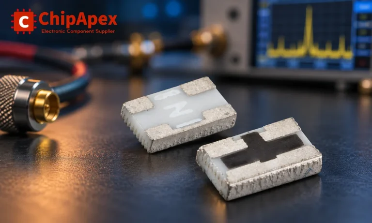
Understand RF attenuator dB values, fixed and programmable types, impedance, power limits and noise tradeoffs before choosing parts for an RF signal path.
Read More
CD4081BCN is listed in the Inverter Gates range at ChipApex. The manufacturer field lists onsemi. Its product description is IC GATE AND 4CH 2-INP…
Read More
CD4081BCN is listed in the Inverter Gates range at ChipApex. The manufacturer field lists onsemi. Its product description is IC GATE AND 4CH 2-INP…
Read More
The activity of extra discounts on wholesale prices is in full swing…
Please fill in your contact information and we will send you the latest wholesale price list.





