 ChipApex | Global Electronic Components Supplier

SEARCH
Search Product
Search Post
— IC芯片 | 连接器 | 传感器 | 被动器件 —
Search productSearch post
— IC芯片 | 连接器 | 传感器 | 被动器件 —
Consult the customer manager about the wholesale price.
consultation hotline:86-132-6715-2157
email:[email protected]
Contact the product manager for consultation. One-stop consultation is available.
Do you want a lower wholesale price? Please send us your inquiry and we will reply immediately.
CDCF2510PWRG4 is listed in the Application Specific Clock/Timing range at ChipApex. The manufacturer field lists Texas Instruments. Its product description is IC 3.3V PLL CLK-DRVR 24-TSSOP. Review the specifications below when checking this part for your BOM.
The CDCF2510PWRG4 is a 3.3-V phase-lock loop (PLL) clock driver manufactured by Texas Instruments, housed in a 24-pin TSSOP package. It operates within a frequency range of 25 MHz to 140 MHz and supports a supply voltage of 3 V to 3.6 V. The device distributes one clock input to ten outputs with low skew and jitter characteristics. Static phase error at 66 MHz to 133 MHz is ±125 ps, while cycle-to-cycle jitter is |70| ps at 66 MHz to 100 MHz and |65| ps at 100 MHz to 133 MHz. It includes integrated series-damping resistors and requires a stabilization time of 1 ms for PLL lock.
Verify that the component matches the exact part number CDCF2510PWRG4, as ordering suffixes may indicate variations in packaging or environmental compliance. Confirm RoHS status and lead finish details against the manufacturer's latest documentation before procurement.
Ensure the application frequency falls between 25 MHz and 140 MHz. Verify that the system can accommodate the required 1 ms stabilization time for the PLL to achieve phase lock after power-up or signal changes. Check that the load capacitance requirements are met to maintain specified jitter and skew performance.
This device belongs to the CDCF2510 family of high-performance, low-skew, low-jitter PLL clock drivers. It is specifically engineered for synchronous DRAM applications where precise phase alignment and minimal jitter are critical for system stability and data integrity.
The CDCVF2510A is documented as a replacement for this device. Verify functional compatibility and pinout correspondence before substitution.
Explore related parts through Clock/Timing, Integrated Circuits (ICs), all product categories, ChipApex homepage.
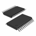 CDCF2510PWRG4

CDCF2510PWRG4 is listed in the Application Specific Clock/Timing range at ChipApex. The manufacturer field lists Texas Instruments. Its product description is IC 3.3V PLL…
Read More
Learn what an integrated circuit is, how ICs work, the main types and the specs to check before choosing a part for your design…
Read More
CDCF2510PWRG4 is listed in the Application Specific Clock/Timing range at ChipApex. The manufacturer field lists Texas Instruments. Its product description is IC 3.3V PLL…
Read More
CDCF2510PWRG4 is listed in the Application Specific Clock/Timing range at ChipApex. The manufacturer field lists Texas Instruments. Its product description is IC 3.3V PLL…
Read More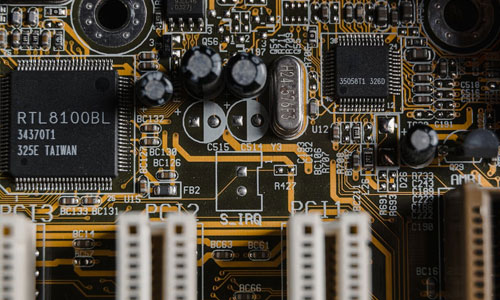
CDCF2510PWRG4 is listed in the Application Specific Clock/Timing range at ChipApex. The manufacturer field lists Texas Instruments. Its product description is IC 3.3V PLL…
Read More
CDCF2510PWRG4 is listed in the Application Specific Clock/Timing range at ChipApex. The manufacturer field lists Texas Instruments. Its product description is IC 3.3V PLL…
Read More
CDCF2510PWRG4 is listed in the Application Specific Clock/Timing range at ChipApex. The manufacturer field lists Texas Instruments. Its product description is IC 3.3V PLL…
Read More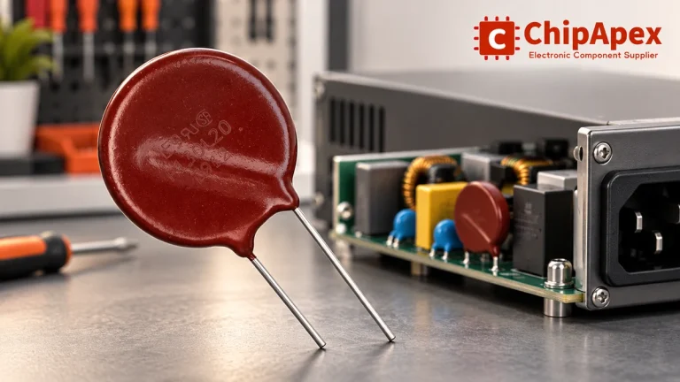
Select MOV varistors by continuous voltage, clamping behavior, surge waveform and repetition. Check thermal disconnection, fuse coordination and replacements.
Read More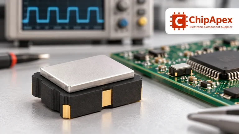
Compare RC, crystal and MEMS oscillator circuits. Check ppm, jitter, load capacitance, startup margin and output compatibility before choosing a clock source.
Read More
CDCF2510PWRG4 is listed in the Application Specific Clock/Timing range at ChipApex. The manufacturer field lists Texas Instruments. Its product description is IC 3.3V PLL…
Read More
CDCF2510PWRG4 is listed in the Application Specific Clock/Timing range at ChipApex. The manufacturer field lists Texas Instruments. Its product description is IC 3.3V PLL…
Read More
Understand how a comparator switches at a voltage threshold, why hysteresis prevents chatter, and which output and input specs matter.
Read More
The activity of extra discounts on wholesale prices is in full swing…
Please fill in your contact information and we will send you the latest wholesale price list.






