 ChipApex | Global Electronic Components Supplier

SEARCH
Search Product
Search Post
— IC芯片 | 连接器 | 传感器 | 被动器件 —
Search productSearch post
— IC芯片 | 连接器 | 传感器 | 被动器件 —
Consult the customer manager about the wholesale price.
consultation hotline:86-132-6715-2157
email:[email protected]
Contact the product manager for consultation. One-stop consultation is available.
Do you want a lower wholesale price? Please send us your inquiry and we will reply immediately.
CDCU2A877NMKT is listed in the Application Specific Clock/Timing range at ChipApex. The manufacturer field lists Texas Instruments. Its product description is 1.8V PHASE-LOCK LOOP CLOCK DRIVE. Review the specifications below when checking this part for your BOM.
The CDCU2A877NMKT is a 1.8-V phase-lock loop clock driver manufactured by Texas Instruments, designed for memory and DDR2 applications. It features a single circuit with a 1:10 input-to-output ratio, supporting differential inputs and outputs. The device operates within a supply voltage range of 1.7 V to 1.9 V and supports a maximum frequency of 410 MHz. It utilizes SSTL-18 signaling standards for both input and output interfaces. The component is housed in a 52-VFBGA package, specifically the MicroStar Junior (7x4.5 mm) form factor, suitable for surface-mount installation. It functions across an operating temperature range from -40°C to +85°C.
Verify component authenticity through authorized distributors or direct manufacturer channels due to potential counterfeit risks. Confirm current availability status as this part may be subject to discontinuation or lifecycle changes. Ensure storage conditions comply with moisture sensitivity level requirements prior to soldering. Validate that the specific package variant matches the design footprint constraints. Review official documentation for any recent product change notifications affecting specifications or pinouts.
Select this component when designing systems requiring a 1.8-V PLL-based clock driver for DDR2 memory interfaces. Ensure the design accommodates the 52-VFBGA MicroStar Junior package dimensions and thermal requirements. Verify compatibility with SSTL-18 signaling standards and differential I/O configurations. Consider the 410 MHz maximum frequency limit relative to system timing needs. Evaluate the -40°C to +85°C operating range against environmental conditions.
This device belongs to the CDCUA877 family of clock drivers from Texas Instruments, specialized for memory applications. It serves as a critical component in distributing reference clocks to multiple memory devices. The family is characterized by low jitter performance and integrated PLL functionality, enabling stable clock generation without external oscillators in many designs.
CDCUA877ZQLT is listed as a similar substitute option.
The maximum operating frequency is 410 MHz.
Yes, it supports differential inputs and differential outputs.
Explore related parts through Clock/Timing, Integrated Circuits (ICs), all product categories, ChipApex homepage.
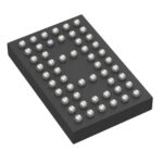 CDCU2A877NMKT

CDCU2A877NMKT is listed in the Application Specific Clock/Timing range at ChipApex. The manufacturer field lists Texas Instruments. Its product description is 1.8V PHASE-LOCK LOOP…
Read More
CDCU2A877NMKT is listed in the Application Specific Clock/Timing range at ChipApex. The manufacturer field lists Texas Instruments. Its product description is 1.8V PHASE-LOCK LOOP…
Read More
CDCU2A877NMKT is listed in the Application Specific Clock/Timing range at ChipApex. The manufacturer field lists Texas Instruments. Its product description is 1.8V PHASE-LOCK LOOP…
Read More
CDCU2A877NMKT is listed in the Application Specific Clock/Timing range at ChipApex. The manufacturer field lists Texas Instruments. Its product description is 1.8V PHASE-LOCK LOOP…
Read More
CDCU2A877NMKT is listed in the Application Specific Clock/Timing range at ChipApex. The manufacturer field lists Texas Instruments. Its product description is 1.8V PHASE-LOCK LOOP…
Read More
CDCU2A877NMKT is listed in the Application Specific Clock/Timing range at ChipApex. The manufacturer field lists Texas Instruments. Its product description is 1.8V PHASE-LOCK LOOP…
Read More
CDCU2A877NMKT is listed in the Application Specific Clock/Timing range at ChipApex. The manufacturer field lists Texas Instruments. Its product description is 1.8V PHASE-LOCK LOOP…
Read More
Choose an AC to DC converter by input range, output demand, isolation, efficiency and thermal derating. Compare architectures and check installation needs.
Read More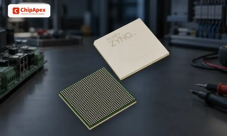
Learn what an integrated circuit is, how ICs work, the main types and the specs to check before choosing a part for your design…
Read More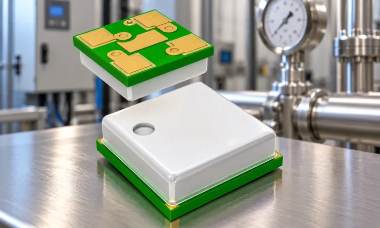
Learn how a pressure transducer converts pressure into voltage, current, or digital output, and compare pressure references and key selection specs.
Read More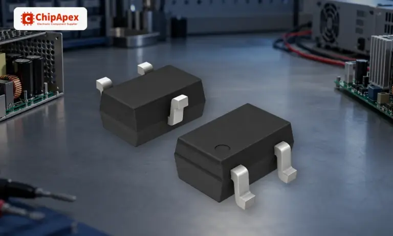
Learn how a diode conducts, how to identify anode and cathode, and when to choose rectifier, TVS, Zener or photodiode types for a circuit.
Read More
CDCU2A877NMKT is listed in the Application Specific Clock/Timing range at ChipApex. The manufacturer field lists Texas Instruments. Its product description is 1.8V PHASE-LOCK LOOP…
Read More
The activity of extra discounts on wholesale prices is in full swing…
Please fill in your contact information and we will send you the latest wholesale price list.





