ChipApex | Global Electronic Components Supplier

SEARCH
Search Product
Search Post
— IC芯片 | 连接器 | 传感器 | 被动器件 —
Search productSearch post
— IC芯片 | 连接器 | 传感器 | 被动器件 —
Consult the customer manager about the wholesale price.
consultation hotline:86-132-6715-2157
email:[email protected]
Contact the product manager for consultation. One-stop consultation is available.
Do you want a lower wholesale price? Please send us your inquiry and we will reply immediately.
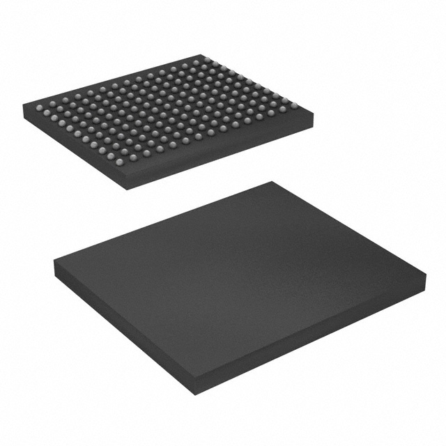
CY7C1263XV18-633BZXC is listed in the Memory IC range at ChipApex. The manufacturer field lists Cypress Semiconductor Corp. Its product description is IC SRAM 36MBIT PAR 165FBGA. Review the specifications below when checking this part for your BOM.
The CY7C1263XV18 is a 36-Mbit QDR II+ Xtreme SRAM with a 2 M × 18 organization. It features a four-word burst architecture and supports a maximum clock frequency of 633 MHz. The device utilizes double data rate interfaces on both read and write ports, transferring data at 1266 MHz. It operates with a core voltage of 1.8 V ± 0.1 V and an I/O voltage range of 1.4 V to 1.6 V. The component is housed in a 165-ball FBGA package measuring 13 × 15 × 1.4 mm.
Verify the specific speed grade suffix matches system timing requirements. Confirm that the I/O supply voltage aligns with the 1.4 V to 1.6 V specification. Ensure the 165-ball FBGA footprint matches the PCB layout. Check for Pb-free compliance if required by environmental standards.
Select this part for applications requiring high bandwidth and low latency. The four-word burst mode is suitable for reducing address bus activity. Consider the 2.5 cycle read latency when designing control logic. Verify power supply constraints for both core and I/O voltages before integration.
This component belongs to the QDR II+ Xtreme family developed by Cypress Semiconductor, now part of Infineon Technologies. It shares architectural similarities with other QDR devices but offers higher clock speeds. The family includes variants with different organizations and speeds, such as the CY7C1265XV18.
CY7C1265XV18: Offers 1 M × 36 organization instead of 2 M × 18. Both share the same package and interface characteristics. Verify width expansion compatibility if replacing with the 36-bit variant.
Asserting DOFF HIGH enables normal QDR II+ Xtreme operation with 2.5 cycle read latency. Asserting it LOW disables the PLL, causing the device to behave like a QDR I device with one cycle read latency.
The ZQ pin is used for impedance matching. An external resistor connected between ZQ and ground tunes the output driver impedance to match the system data bus.
Explore related parts through Memory, Integrated Circuits (ICs), all product categories, ChipApex homepage.
 CY7C1263XV18-633BZXC
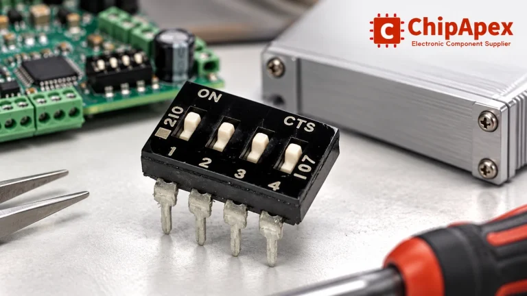
Choose a DIP switch by contact type, coded positions, footprint and signal ratings. Check logic polarity, assembly conditions and PCB configuration behavior.
Read More
CY7C1263XV18-633BZXC is listed in the Memory IC range at ChipApex. The manufacturer field lists Cypress Semiconductor Corp. Its product description is IC SRAM 36MBIT…
Read More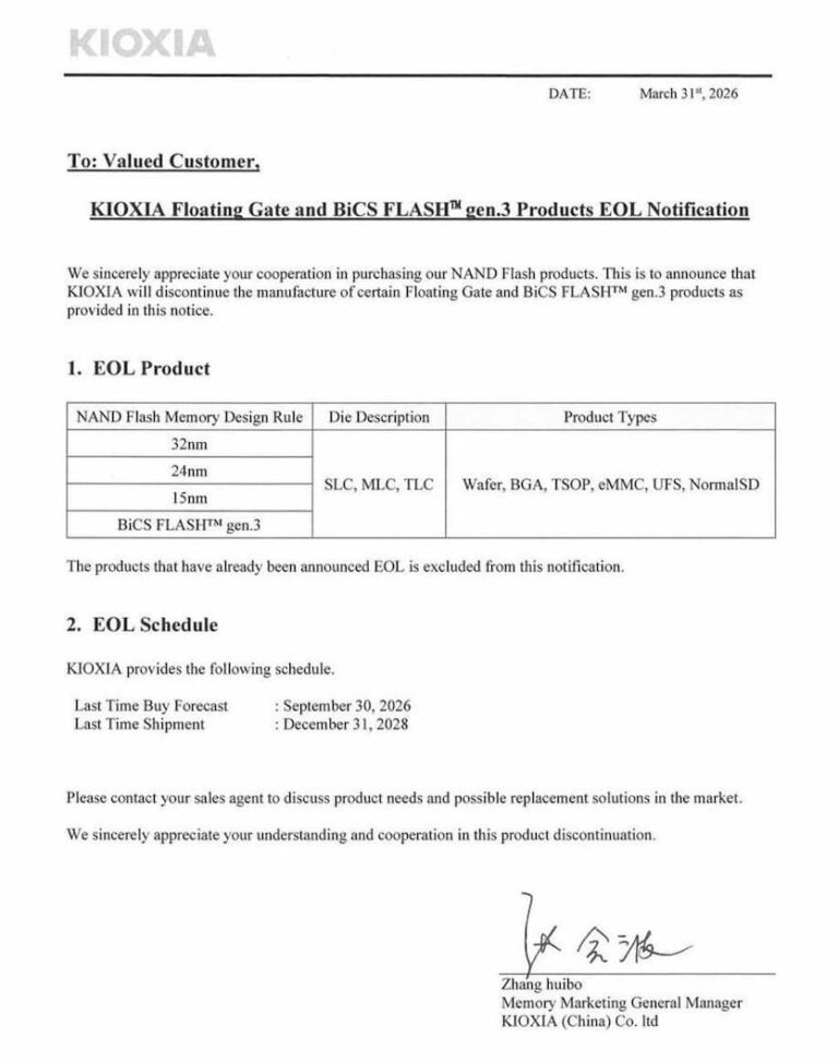
CY7C1263XV18-633BZXC is listed in the Memory IC range at ChipApex. The manufacturer field lists Cypress Semiconductor Corp. Its product description is IC SRAM 36MBIT…
Read More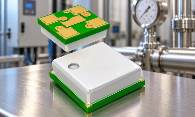
Learn how a pressure transducer converts pressure into voltage, current, or digital output, and compare pressure references and key selection specs.
Read More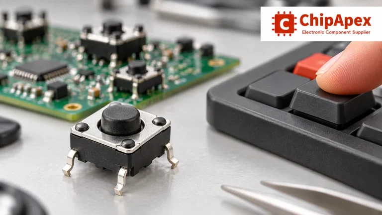
Understand tactile switches, PCB and keyboard differences, four-pin wiring, debounce, force, travel and replacement checks for reliable control inputs.
Read More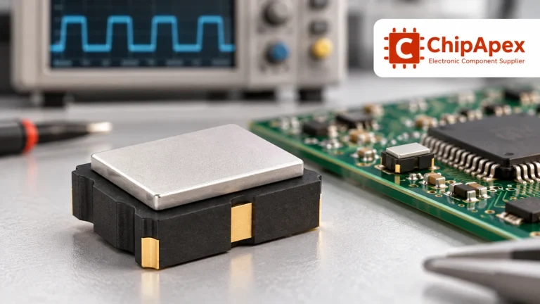
Compare RC, crystal and MEMS oscillator circuits. Check ppm, jitter, load capacitance, startup margin and output compatibility before choosing a clock source.
Read More
CY7C1263XV18-633BZXC is listed in the Memory IC range at ChipApex. The manufacturer field lists Cypress Semiconductor Corp. Its product description is IC SRAM 36MBIT…
Read More
CY7C1263XV18-633BZXC is listed in the Memory IC range at ChipApex. The manufacturer field lists Cypress Semiconductor Corp. Its product description is IC SRAM 36MBIT…
Read More
CY7C1263XV18-633BZXC is listed in the Memory IC range at ChipApex. The manufacturer field lists Cypress Semiconductor Corp. Its product description is IC SRAM 36MBIT…
Read More
CY7C1263XV18-633BZXC is listed in the Memory IC range at ChipApex. The manufacturer field lists Cypress Semiconductor Corp. Its product description is IC SRAM 36MBIT…
Read More
CY7C1263XV18-633BZXC is listed in the Memory IC range at ChipApex. The manufacturer field lists Cypress Semiconductor Corp. Its product description is IC SRAM 36MBIT…
Read More
CY7C1263XV18-633BZXC is listed in the Memory IC range at ChipApex. The manufacturer field lists Cypress Semiconductor Corp. Its product description is IC SRAM 36MBIT…
Read More
The activity of extra discounts on wholesale prices is in full swing…
Please fill in your contact information and we will send you the latest wholesale price list.