ChipApex | Global Electronic Components Supplier

SEARCH
Search Product
Search Post
— IC芯片 | 连接器 | 传感器 | 被动器件 —
Search productSearch post
— IC芯片 | 连接器 | 传感器 | 被动器件 —
Consult the customer manager about the wholesale price.
consultation hotline:86-132-6715-2157
email:[email protected]
Contact the product manager for consultation. One-stop consultation is available.
Do you want a lower wholesale price? Please send us your inquiry and we will reply immediately.
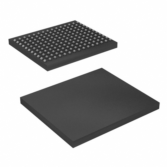
CY7C1568KV18-500BZXI is listed in the Memory IC range at ChipApex. The manufacturer field lists Infineon Technologies. Its product description is IC SRAM 72MBIT PAR 165FBGA. Review the specifications below when checking this part for your BOM.
The CY7C1568KV18-500BZXI is a 72-Mbit DDR II+ synchronous SRAM organized as 4M x 18. It supports a maximum operating frequency of 500 MHz, providing high bandwidth for data-intensive applications. The device features a two-word burst architecture with a 2.5-cycle read latency when the DOFF pin is asserted HIGH. It operates within a core voltage range of 1.7 V to 1.9 V and an I/O voltage range of 1.4 V to VDD. The component utilizes a 165-ball fine pitch ball grid array (FBGA) package measuring 13 x 15 x 1.4 mm.
Verify the exact speed grade suffix matches the required operational frequency, as the base model number may cover multiple clock speeds. Confirm the package type corresponds to the 165-ball FBGA configuration. Ensure the ordering suffix aligns with the desired lead-free status and industrial temperature rating specifications provided by the manufacturer.
Select this component for designs requiring high throughput with a two-word burst capability. Consider the 2.5-cycle read latency when designing the system interface logic. Evaluate the need for echo clocks and valid data indicators to manage signal integrity at high frequencies. Verify compatibility with HSTL input and output buffer standards for the target application environment.
This part belongs to the Cypress/Infineon DDR II+ SRAM family, which offers advanced synchronous peripheral circuitry integrated with an SRAM core. The series provides options for varying densities and organizations, including 4M x 18 and 2M x 36 configurations. These devices are designed for applications needing high-performance memory solutions with low power consumption characteristics.
The CY7C1570KV18 serves as a functional alternative within the same datasheet, offering a 2M x 36 organization instead of 4M x 18. Both parts share identical electrical characteristics and package dimensions, allowing for potential width expansion or density adaptation in compatible system designs.
When the DOFF pin is asserted HIGH, the device operates with a 2.5-cycle read latency. If DOFF is asserted LOW, the device behaves like a DDR I device with a 1-cycle read latency.
The ZQ pin is used for output impedance matching. An external resistor connected between ZQ and ground tunes the device outputs to the system data bus impedance, ensuring signal integrity.
Explore related parts through Memory, Integrated Circuits (ICs), all product categories, ChipApex homepage.
 CY7C1568KV18-500BZXI
 is listed in the Memory IC range at ChipApex. The manufacturer field lists Infineon Technologies. Its product description is IC SRAM 72MBIT PAR…
Read More
CY7C1568KV18-500BZXI is listed in the Memory IC range at ChipApex. The manufacturer field lists Infineon Technologies. Its product description is IC SRAM 72MBIT PAR…
Read More
CY7C1568KV18-500BZXI is listed in the Memory IC range at ChipApex. The manufacturer field lists Infineon Technologies. Its product description is IC SRAM 72MBIT PAR…
Read More
CY7C1568KV18-500BZXI is listed in the Memory IC range at ChipApex. The manufacturer field lists Infineon Technologies. Its product description is IC SRAM 72MBIT PAR…
Read More
CY7C1568KV18-500BZXI is listed in the Memory IC range at ChipApex. The manufacturer field lists Infineon Technologies. Its product description is IC SRAM 72MBIT PAR…
Read More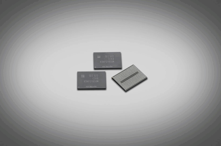
CY7C1568KV18-500BZXI is listed in the Memory IC range at ChipApex. The manufacturer field lists Infineon Technologies. Its product description is IC SRAM 72MBIT PAR…
Read More
CY7C1568KV18-500BZXI is listed in the Memory IC range at ChipApex. The manufacturer field lists Infineon Technologies. Its product description is IC SRAM 72MBIT PAR…
Read More
Understand how a comparator switches at a voltage threshold, why hysteresis prevents chatter, and which output and input specs matter.
Read More
CY7C1568KV18-500BZXI is listed in the Memory IC range at ChipApex. The manufacturer field lists Infineon Technologies. Its product description is IC SRAM 72MBIT PAR…
Read More
CY7C1568KV18-500BZXI is listed in the Memory IC range at ChipApex. The manufacturer field lists Infineon Technologies. Its product description is IC SRAM 72MBIT PAR…
Read More
See how a MEMS gyroscope measures angular rate, why its angle estimate drifts, and which range, noise, interface and temperature specs to compare.
Read More
CY7C1568KV18-500BZXI is listed in the Memory IC range at ChipApex. The manufacturer field lists Infineon Technologies. Its product description is IC SRAM 72MBIT PAR…
Read More
The activity of extra discounts on wholesale prices is in full swing…
Please fill in your contact information and we will send you the latest wholesale price list.