 ChipApex | Global Electronic Components Supplier

SEARCH
Search Product
Search Post
— IC芯片 | 连接器 | 传感器 | 被动器件 —
Search productSearch post
— IC芯片 | 连接器 | 传感器 | 被动器件 —
Consult the customer manager about the wholesale price.
consultation hotline:86-132-6715-2157
email:[email protected]
Contact the product manager for consultation. One-stop consultation is available.
Do you want a lower wholesale price? Please send us your inquiry and we will reply immediately.
CY7C4231V-25AXC is listed in the FIFOs Memory range at ChipApex. The manufacturer field lists Infineon Technologies. Its product description is IC FIFO SYNC 2KX9 15NS 32TQFP. Review the specifications below when checking this part for your BOM.
The CY7C4231V-25AXC is a low-voltage, high-speed synchronous FIFO memory with a density of 2K x 9 bits. It operates at a maximum frequency of 40 MHz with a minimum cycle time of 25 ns and an access time of 15 ns. The device functions on a 3.3 V supply with active current consumption of 20 mA. It features independent read and write clocks, programmable Almost Full/Empty flags, and 5V-tolerant inputs. The component is housed in a 32-pin Pb-Free Thin Quad Flatpack (A32) package.
Verify the specific suffix 'AXC' confirms the Pb-Free Thin Quad Flatpack (A32) package type and commercial temperature range. Ensure the ordering code matches the required 25 ns speed grade. Confirm RoHS compliance status if required by local regulations. Cross-reference the manufacturer's latest datasheet revision to validate pinout and electrical characteristics against current production standards.
Select this component when a 2K depth with 9-bit width is required for asynchronous data transfer between clock domains. The 25 ns speed grade suits applications operating up to 40 MHz. Consider the industrial temperature variant if ambient conditions exceed standard commercial limits. Verify that the 3.3 V logic level compatibility aligns with the target system voltage requirements.
This part belongs to the CY7C42X1V family of low-voltage synchronous FIFOs manufactured by Cypress Semiconductor, now part of Infineon Technologies. The family includes variants ranging from 64x9 to 8Kx9 densities. The CY7C4231V specifically provides 2048 words of storage, bridging the gap between smaller 1K buffers and larger 4K or 8K configurations.
CY7C4231V-25AC serves as a non-Pb-Free equivalent within the same package footprint. CY7C4231V-15AXC offers faster performance but requires verification of timing constraints. Direct substitutes from other manufacturers require careful evaluation of pin compatibility and electrical specifications.
The offset registers are programmed by holding WEN2/LD LOW during reset and using subsequent write clock cycles to load data into the empty and full offset LSB and MSB registers.
WEN2/LD acts as a dual-purpose pin: it serves as a second write enable when held HIGH at reset, or as a load control for programming flag offsets when held LOW at reset.
Explore related parts through Logic, Integrated Circuits (ICs), all product categories, ChipApex homepage.
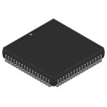 CY7C4231V-25AXC
Choose an AC to DC converter by input range, output demand, isolation, efficiency and thermal derating. Compare architectures and check installation needs.
Read More
Learn the relay definition, coil and contact operation, NO and NC forms, load ratings and suppression choices. Compare mechanical, reed and solid-state types.
Read More
CY7C4231V-25AXC is listed in the FIFOs Memory range at ChipApex. The manufacturer field lists Infineon Technologies. Its product description is IC FIFO SYNC 2KX9…
Read More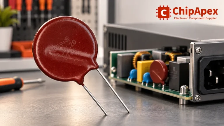
Select MOV varistors by continuous voltage, clamping behavior, surge waveform and repetition. Check thermal disconnection, fuse coordination and replacements.
Read More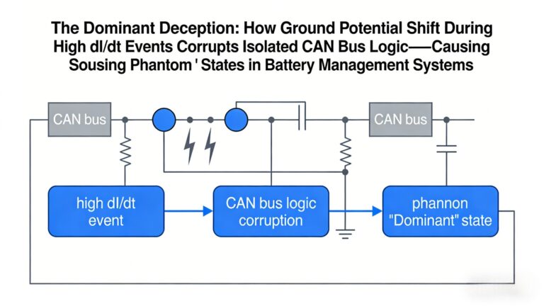
CY7C4231V-25AXC is listed in the FIFOs Memory range at ChipApex. The manufacturer field lists Infineon Technologies. Its product description is IC FIFO SYNC 2KX9…
Read More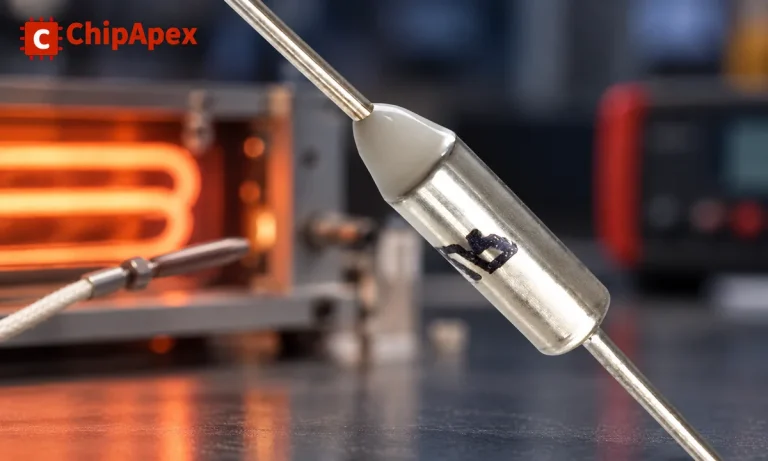
Understand thermal fuse operation, Tf, Th and Tm, electrical ratings and mounting. Check temperature limits and replacement requirements for your design.
Read More
CY7C4231V-25AXC is listed in the FIFOs Memory range at ChipApex. The manufacturer field lists Infineon Technologies. Its product description is IC FIFO SYNC 2KX9…
Read More
CY7C4231V-25AXC is listed in the FIFOs Memory range at ChipApex. The manufacturer field lists Infineon Technologies. Its product description is IC FIFO SYNC 2KX9…
Read More
CY7C4231V-25AXC is listed in the FIFOs Memory range at ChipApex. The manufacturer field lists Infineon Technologies. Its product description is IC FIFO SYNC 2KX9…
Read More
Learn how a pressure transducer converts pressure into voltage, current, or digital output, and compare pressure references and key selection specs.
Read More
CY7C4231V-25AXC is listed in the FIFOs Memory range at ChipApex. The manufacturer field lists Infineon Technologies. Its product description is IC FIFO SYNC 2KX9…
Read More
Choose a rocker switch by AC/DC ratings, contact arrangement, illumination, panel fit and sealing. Get practical checks for engineering and component sourcing.
Read More
The activity of extra discounts on wholesale prices is in full swing…
Please fill in your contact information and we will send you the latest wholesale price list.





