 ChipApex | Global Electronic Components Supplier

SEARCH
Search Product
Search Post
— IC芯片 | 连接器 | 传感器 | 被动器件 —
Search productSearch post
— IC芯片 | 连接器 | 传感器 | 被动器件 —
Consult the customer manager about the wholesale price.
consultation hotline:86-132-6715-2157
email:[email protected]
Contact the product manager for consultation. One-stop consultation is available.
Do you want a lower wholesale price? Please send us your inquiry and we will reply immediately.
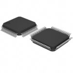
CY7C4245V-25ASXC is listed in the FIFOs Memory range at ChipApex. The manufacturer field lists Infineon Technologies. Its product description is IC FIFO SYNC 4KX18 15NS 64TQFP. Review the specifications below when checking this part for your BOM.
The CY7C4245V-25ASXC is a low-voltage synchronous FIFO memory with a 4K x 18 organization and an 18-bit data bus. It operates at 3.3V with a maximum frequency of 40 MHz and a minimum cycle time of 25 ns. The device features independent read and write clocks, programmable Almost Full/Empty flags, and supports depth expansion via cascade pins. It is housed in a 64-pin 10x10 mm STQFP package.
Verify the specific suffix 'ASXC' against official Infineon documentation to confirm package type and temperature range. Ensure compatibility with 3.3V logic levels and check for lead-free compliance requirements. Confirm availability as this component series may have end-of-life status or be superseded by newer generations.
Select this component when a 4K depth and 18-bit width are required for synchronous buffering. Consider the 25 ns speed grade for applications needing up to 40 MHz operation. Evaluate the need for programmable flags and depth expansion capabilities before choosing between other densities in the CY7C42X5V family.
This part belongs to the CY7C42X5V family of low-voltage synchronous FIFOs manufactured by Cypress Semiconductor, now part of Infineon Technologies. The family offers various densities from 64x18 to 4Kx18, sharing common pinouts and functional architectures while differing in storage capacity and speed grades.
Check for direct substitutes within the CY7C42X5V family with different speed grades (e.g., -15 or -35) if timing constraints allow. Verify if newer Infineon FIFO products offer compatible pinouts and functionality.
The flags become synchronous to the Write Clock (WCLK) or Read Clock (RCLK) respectively when the VCC/SMODE pin is tied to VSS. If tied to VCC, they operate asynchronously.
In standalone mode, it serves as the Retransmit input to reset the read pointer. In depth expansion configurations, it designates the first device in the daisy chain when tied to VSS.
Explore related parts through Logic, Integrated Circuits (ICs), all product categories, ChipApex homepage.
 CY7C4245V-25ASXC
CY7C4245V-25ASXC is listed in the FIFOs Memory range at ChipApex. The manufacturer field lists Infineon Technologies. Its product description is IC FIFO SYNC 4KX18…
Read More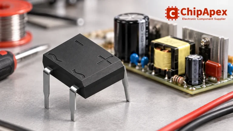
Select a bridge rectifier by reverse voltage, capacitor charging current, startup surge and cooling. Work through a stated DC voltage and ripple example.
Read More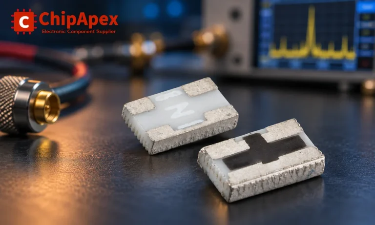
Understand RF attenuator dB values, fixed and programmable types, impedance, power limits and noise tradeoffs before choosing parts for an RF signal path.
Read More
CY7C4245V-25ASXC is listed in the FIFOs Memory range at ChipApex. The manufacturer field lists Infineon Technologies. Its product description is IC FIFO SYNC 4KX18…
Read More
Select power transformers by input frequency, secondary VA, rectifier load, isolation, regulation and inrush. Build a clearer specification for your next RFQ.
Read More
CY7C4245V-25ASXC is listed in the FIFOs Memory range at ChipApex. The manufacturer field lists Infineon Technologies. Its product description is IC FIFO SYNC 4KX18…
Read More
CY7C4245V-25ASXC is listed in the FIFOs Memory range at ChipApex. The manufacturer field lists Infineon Technologies. Its product description is IC FIFO SYNC 4KX18…
Read More
Learn what an integrated circuit is, how ICs work, the main types and the specs to check before choosing a part for your design…
Read More
CY7C4245V-25ASXC is listed in the FIFOs Memory range at ChipApex. The manufacturer field lists Infineon Technologies. Its product description is IC FIFO SYNC 4KX18…
Read More
CY7C4245V-25ASXC is listed in the FIFOs Memory range at ChipApex. The manufacturer field lists Infineon Technologies. Its product description is IC FIFO SYNC 4KX18…
Read More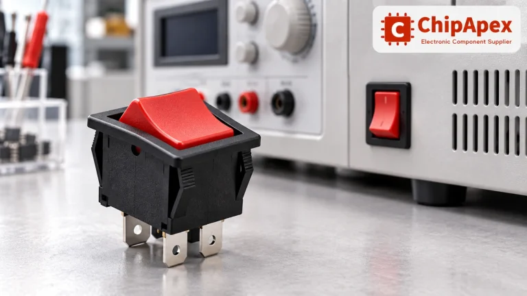
Choose a rocker switch by AC/DC ratings, contact arrangement, illumination, panel fit and sealing. Get practical checks for engineering and component sourcing.
Read More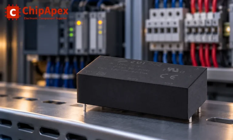
Choose an AC to DC converter by input range, output demand, isolation, efficiency and thermal derating. Compare architectures and check installation needs.
Read More
The activity of extra discounts on wholesale prices is in full swing…
Please fill in your contact information and we will send you the latest wholesale price list.





