 ChipApex | Global Electronic Components Supplier

SEARCH
Search Product
Search Post
— IC芯片 | 连接器 | 传感器 | 被动器件 —
Search productSearch post
— IC芯片 | 连接器 | 传感器 | 被动器件 —
Consult the customer manager about the wholesale price.
consultation hotline:86-132-6715-2157
email:[email protected]
Contact the product manager for consultation. One-stop consultation is available.
Do you want a lower wholesale price? Please send us your inquiry and we will reply immediately.
CY7C4261-15JXC is listed in the FIFOs Memory range at ChipApex. The manufacturer field lists Infineon Technologies. Its product description is IC FIFO SYNC 16KX9 10NS 32PLCC. Review the specifications below when checking this part for your BOM.
The CY7C4261-15JXC is a 16K x 9 synchronous FIFO memory fabricated using 0.5 micron CMOS technology. It features independent read and write clocks, supporting maximum frequencies of 66.7 MHz with a 10 ns access time. The device operates on a single 5V supply with an active current of 35 mA. It includes programmable Almost Full and Almost Empty flags, TTL-compatible inputs, and center power/ground pins for noise reduction. The component is housed in a 32-pin Plastic Leaded Chip Carrier (PLCC) package.
Verify the specific ordering suffix 'JXC' confirms the lead-free (Pb-Free) 32-pin PLCC package variant. Confirm the manufacturer source, as Cypress Semiconductor was acquired by Infineon Technologies. Ensure the commercial temperature range specification aligns with the target application environment requirements.
Select this model for applications requiring 16K depth and 9-bit word width. Choose the -15 speed grade for 66.7 MHz operation. Consider the CY7C4271 if 32K depth is required. Verify compatibility with existing system voltage levels and clocking architectures before integration.
This component belongs to the CY7C4261/71 Deep Sync FIFO family. It serves as a density upgrade option for legacy IDT72201/11/21/31/41/51 series parts. The device maintains pin compatibility within its family while offering optimized speed and power characteristics through advanced CMOS fabrication processes.
Pin-compatible alternatives include the CY7C4271 for increased depth or other speed grades within the same package. Legacy replacements may include the IDT72201/11/21/31/41/51 series, subject to verification of electrical parameter alignment.
These flags are configured by writing offset values into internal registers. This is done by holding WEN2/LD LOW during reset and using subsequent clock cycles to load the empty and full offset registers.
If held HIGH at reset, it acts as a second write enable for depth expansion. If held LOW at reset, it functions as a Load (LD) enable to program the flag offset registers.
Explore related parts through Logic, Integrated Circuits (ICs), all product categories, ChipApex homepage.
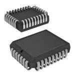 CY7C4261-15JXC

CY7C4261-15JXC is listed in the FIFOs Memory range at ChipApex. The manufacturer field lists Infineon Technologies. Its product description is IC FIFO SYNC 16KX9…
Read More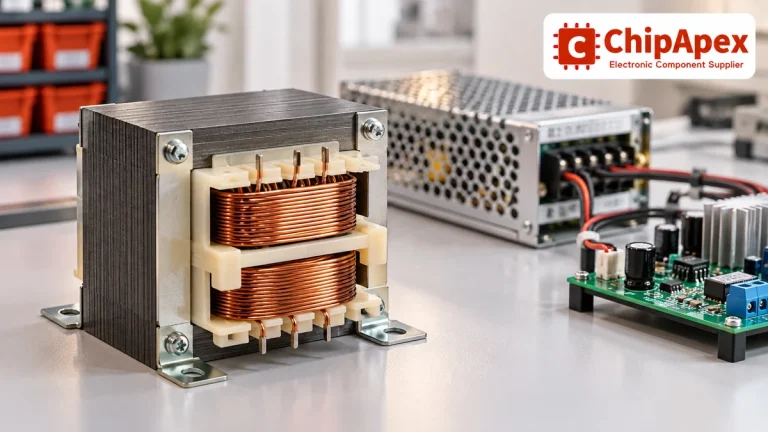
Select power transformers by input frequency, secondary VA, rectifier load, isolation, regulation and inrush. Build a clearer specification for your next RFQ.
Read More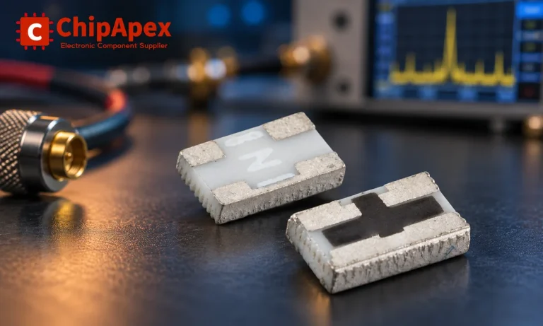
Understand RF attenuator dB values, fixed and programmable types, impedance, power limits and noise tradeoffs before choosing parts for an RF signal path.
Read More
CY7C4261-15JXC is listed in the FIFOs Memory range at ChipApex. The manufacturer field lists Infineon Technologies. Its product description is IC FIFO SYNC 16KX9…
Read More
CY7C4261-15JXC is listed in the FIFOs Memory range at ChipApex. The manufacturer field lists Infineon Technologies. Its product description is IC FIFO SYNC 16KX9…
Read More
Understand voltage controlled oscillator tuning, phase noise and PLL operation. Check supply noise, output loading and requirements before selection.
Read More
Learn how to use ferrite beads for noise filtering. Check impedance, DC bias, placement, resonance and load-step behavior before selecting a part.
Read More
CY7C4261-15JXC is listed in the FIFOs Memory range at ChipApex. The manufacturer field lists Infineon Technologies. Its product description is IC FIFO SYNC 16KX9…
Read More
Learn how an analog front end conditions sensor signals. Compare gain, noise, filtering, ADC settling and integration options before selecting components.
Read More
CY7C4261-15JXC is listed in the FIFOs Memory range at ChipApex. The manufacturer field lists Infineon Technologies. Its product description is IC FIFO SYNC 16KX9…
Read More
CY7C4261-15JXC is listed in the FIFOs Memory range at ChipApex. The manufacturer field lists Infineon Technologies. Its product description is IC FIFO SYNC 16KX9…
Read More
Learn how CPLDs implement hardware logic, compare them with FPGAs and MCUs, and check timing, I/O voltage, startup behavior and programming requirements.
Read More
The activity of extra discounts on wholesale prices is in full swing…
Please fill in your contact information and we will send you the latest wholesale price list.





