 ChipApex | Global Electronic Components Supplier

SEARCH
Search Product
Search Post
— IC芯片 | 连接器 | 传感器 | 被动器件 —
Search productSearch post
— IC芯片 | 连接器 | 传感器 | 被动器件 —
Consult the customer manager about the wholesale price.
consultation hotline:86-132-6715-2157
email:[email protected]
Contact the product manager for consultation. One-stop consultation is available.
Do you want a lower wholesale price? Please send us your inquiry and we will reply immediately.
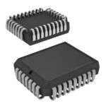
CY7C4291-10JXC is listed in the FIFOs Memory range at ChipApex. The manufacturer field lists Infineon Technologies. Its product description is IC FIFO SYNC 128KX9 8NS 32PLCC. Review the specifications below when checking this part for your BOM.
The CY7C4291-10JXC is a 128K x 9 Deep Synchronous FIFO memory manufactured by Infineon Technologies (formerly Cypress Semiconductor). It operates at a maximum frequency of 100 MHz with a cycle time of 10 ns. The device utilizes 0.5-micron CMOS technology and features independent read and write clocks. It includes programmable Almost Empty and Almost Full flags, TTL-compatible inputs, and center power/ground pins for noise reduction.
Verify the component is sourced from authorized distributors to ensure authenticity. Confirm the package type matches the J65 specification. Check for RoHS compliance markings corresponding to the Pb-Free suffix. Validate that the operating temperature range meets commercial requirements.
Select this model for applications requiring 128K depth and 9-bit word width. Ensure the system supports independent read and write clock signals. Verify voltage compatibility with 5V logic levels. Consider the 32-pin PLCC package constraints for PCB layout.
This component belongs to the CY7C42X1 family of deep synchronous FIFOs. It offers pin-compatible density upgrades within the series. The device is designed for high-speed buffering in digital signal processing and communication networks.
Pin-compatible substitutes include IDT72201, IDT72211, IDT72221, IDT72231, IDT72241, and IDT72251 families. Verify electrical specifications and timing parameters before substitution.
The Almost Empty and Almost Full flags are programmed via the WEN2/LD and WCLK pins during reset or specific control sequences.
Yes, the RCLK and WCLK can be tied together for single-clock operation or run independently for asynchronous applications.
Explore related parts through Logic, Integrated Circuits (ICs), all product categories, ChipApex homepage.
 CY7C4291-10JXC

CY7C4291-10JXC is listed in the FIFOs Memory range at ChipApex. The manufacturer field lists Infineon Technologies. Its product description is IC FIFO SYNC 128KX9…
Read More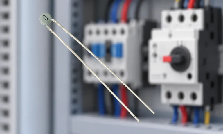
Learn why PTC resistance rises with temperature, how it differs from NTC, and which ratings matter for sensing and protection.
Read More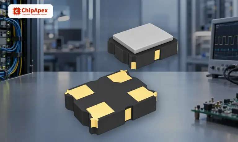
Understand how oscillators generate timing signals, how they differ from crystals, and which frequency, output and stability specs matter when choosing one.
Read More
CY7C4291-10JXC is listed in the FIFOs Memory range at ChipApex. The manufacturer field lists Infineon Technologies. Its product description is IC FIFO SYNC 128KX9…
Read More
CY7C4291-10JXC is listed in the FIFOs Memory range at ChipApex. The manufacturer field lists Infineon Technologies. Its product description is IC FIFO SYNC 128KX9…
Read More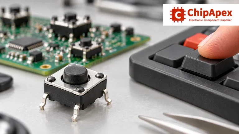
Understand tactile switches, PCB and keyboard differences, four-pin wiring, debounce, force, travel and replacement checks for reliable control inputs.
Read More
CY7C4291-10JXC is listed in the FIFOs Memory range at ChipApex. The manufacturer field lists Infineon Technologies. Its product description is IC FIFO SYNC 128KX9…
Read More
CY7C4291-10JXC is listed in the FIFOs Memory range at ChipApex. The manufacturer field lists Infineon Technologies. Its product description is IC FIFO SYNC 128KX9…
Read More
CY7C4291-10JXC is listed in the FIFOs Memory range at ChipApex. The manufacturer field lists Infineon Technologies. Its product description is IC FIFO SYNC 128KX9…
Read More
CY7C4291-10JXC is listed in the FIFOs Memory range at ChipApex. The manufacturer field lists Infineon Technologies. Its product description is IC FIFO SYNC 128KX9…
Read More
CY7C4291-10JXC is listed in the FIFOs Memory range at ChipApex. The manufacturer field lists Infineon Technologies. Its product description is IC FIFO SYNC 128KX9…
Read More
CY7C4291-10JXC is listed in the FIFOs Memory range at ChipApex. The manufacturer field lists Infineon Technologies. Its product description is IC FIFO SYNC 128KX9…
Read More
The activity of extra discounts on wholesale prices is in full swing…
Please fill in your contact information and we will send you the latest wholesale price list.







