 ChipApex | Global Electronic Components Supplier
DG408DQ-E3
Search Product
Search Post
— IC芯片 | 连接器 | 传感器 | 被动器件 —
Search productSearch post
— IC芯片 | 连接器 | 传感器 | 被动器件 —
Consult the customer manager about the wholesale price.
consultation hotline:86-132-6715-2157
email:[email protected]
Contact the product manager for consultation. One-stop consultation is available.
Do you want a lower wholesale price? Please send us your inquiry and we will reply immediately.
The DG408DQ-E3 is an 8-channel single-ended analog multiplexer manufactured by Vishay Siliconix. It connects one of eight inputs to a common output based on a 3-bit binary address (A0, A1, A2). The device operates with a single supply voltage ranging from +5 V to +36 V or dual supplies from ±5 V to ±20 V. Key electrical parameters include a maximum drain-source on-resistance of 100 Ω, a transition time of 160 ns, and a charge injection of 20 pC. It features TTL-compatible logic inputs and an enable function for stacking multiple devices. The component is housed in a 16-pin TSSOP package and supports an operating temperature range from -40 °C to +85 °C.
Verify that the ordering suffix matches the required configuration. The '-E3' designation indicates lead-free and RoHS-compliant terminations. Confirm the 'DQ' suffix corresponds to the 16-pin TSSOP package variant. Ensure the specific part number aligns with commercial temperature ratings before procurement.
Select this component when an 8:1 single-ended multiplexing configuration is required. It is suitable for applications needing low charge injection and fast transition times. Verify that the system voltage requirements fall within the specified single or dual supply ranges. Consider the TSSOP package dimensions for PCB layout constraints.
This component belongs to the DG408/DG409 family of high-performance CMOS analog multiplexers. The DG408 provides an 8-channel single-ended configuration, while the DG409 offers a dual 4-channel differential setup. Both share similar performance characteristics and are designed using a 44 V silicon-gate CMOS process.
Publicly confirmed substitute part numbers are not available in the provided documentation. Cross-referencing requires verifying pinout compatibility, on-resistance limits, and package dimensions against alternative manufacturers' offerings.
The Enable function allows the user to reset all switches to the off state, which facilitates stacking several devices together.
Signals on source or drain pins exceeding the power supply rails are clamped by internal diodes. External blocking diodes can also be added for additional protection.
The typical charge injection is 20 pC, measured with a load capacitance of 10 nF and the source at 0 V.
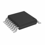 DG408DQ-E3
The activity of extra discounts on wholesale prices is in full swing…
Please fill in your contact information and we will send you the latest wholesale price list.





