 ChipApex | Global Electronic Components Supplier
DG412CUE+
Search Product
Search Post
— IC芯片 | 连接器 | 传感器 | 被动器件 —
Search productSearch post
— IC芯片 | 连接器 | 传感器 | 被动器件 —
Consult the customer manager about the wholesale price.
consultation hotline:86-132-6715-2157
email:[email protected]
Contact the product manager for consultation. One-stop consultation is available.
Do you want a lower wholesale price? Please send us your inquiry and we will reply immediately.
The DG412CUE+ is a quad, single-pole/single-throw (SPST) analog switch from the Maxim DG411/DG412/DG413 family. It features a normally open configuration and operates on a single +10V to +30V supply or bipolar ±4.5V to ±20V supplies. The device provides a maximum on-resistance of 45Ω, an on-resistance match between channels of 3Ω max, and guaranteed on-resistance flatness of Δ4Ω max over the signal range. It exhibits low charge injection of 10pC max, off-leakage current less than 5nA at +85°C, and turn-on/turn-off times under 175ns/145ns respectively. Packaged in a 16-pin TSSOP, it supports rail-to-rail signal handling and TTL/CMOS logic compatibility.
Verify the specific ordering suffix against official manufacturer documentation to confirm package type and temperature range. Confirm RoHS compliance status directly with the supplier or datasheet revision history before procurement. Ensure the component meets all absolute maximum ratings for your specific power supply sequencing requirements.
Select this part when a normally open analog switching topology is required within the DG41x family. Verify that the operating voltage range aligns with your system's single or dual supply rails. Consider the 45Ω maximum on-resistance and 10pC charge injection limits relative to your signal integrity requirements.
This component belongs to the DG411/DG412/DG413 series of improved quad SPST analog switches. The 'DG412' designation specifically indicates a normally open switch configuration, distinguishing it from the normally closed DG411 and the mixed NC/NO DG413 variants. All three share identical pinouts and core electrical characteristics.
Direct functional replacements within the same family include the DG411CUE+ (normally closed) and DG413CUE+ (mixed configuration). These parts share the same 16-pin TSSOP footprint and electrical specifications but differ in internal switch logic states.
The DG412 is a normally open (NO) switch, meaning the channel is open when the logic input is low. The DG411 is a normally closed (NC) switch, where the channel is closed when the logic input is low.
Signals on source or drain pins exceeding the supply rails are clamped by internal diodes. For external protection without affecting leakage, two small signal diodes can be added in series with the supply pins.
The device guarantees an on-resistance flatness (ΔRDS(ON)) of 4Ω maximum over the entire analog signal range.
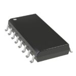 DG412CUE+
The activity of extra discounts on wholesale prices is in full swing…
Please fill in your contact information and we will send you the latest wholesale price list.





