 ChipApex | Global Electronic Components Supplier
FST3306MTCX
Search Product
Search Post
— IC芯片 | 连接器 | 传感器 | 被动器件 —
Search productSearch post
— IC芯片 | 连接器 | 传感器 | 被动器件 —
Consult the customer manager about the wholesale price.
consultation hotline:86-132-6715-2157
email:[email protected]
Contact the product manager for consultation. One-stop consultation is available.
Do you want a lower wholesale price? Please send us your inquiry and we will reply immediately.
The FST3306MTCX is a 2-bit ultra high-speed CMOS FET bus switch manufactured by onsemi. It features TTL-compatible active LOW control inputs and overvoltage tolerant logic. The device provides minimal propagation delay and zero bounce in flow-through mode. It operates within a supply voltage range of 4.0V to 5.5V and an ambient temperature range of -40°C to +85°C. The typical on-resistance is 3Ω at 5.0V VCC, with a maximum of 7Ω under specific conditions. The package is an 8-lead Thin Shrink Small Outline Package (TSSOP).
Verify the component authenticity against the official datasheet specifications. Confirm the package type matches the 8-lead TSSOP outline. Ensure the operating voltage and temperature ranges align with system requirements. Check for RoHS compliance documentation if required by the manufacturing process. Validate that the ordering code suffix corresponds to the tape and reel configuration.
Select this component for designs requiring bidirectional bus switching with low on-resistance. Consider the 2-bit organization for compact signal routing solutions. Evaluate the overvoltage tolerance of control inputs for mixed-voltage environments. Assess the power dissipation limits relative to the thermal resistance of the TSSOP package. Verify compatibility with the target logic family voltage levels.
This device belongs to the FST series of bus switches, designed for high-speed digital signal transmission. It serves as a bridge between different logic domains, allowing flexible interconnection of buses. The FST3306 specifically addresses the need for low-power, high-performance switching in portable and consumer devices.
Consult official replacement lists for equivalent 2-bit bus switches. Verify pinout compatibility and electrical characteristics before substitution. Ensure the alternative device meets the same voltage and temperature specifications.
The Bus Enable (BE) pin controls the switch state. When BE is LOW, Port A is connected to Port B. When BE is HIGH, the switch is open, creating a high-impedance state between the ports.
Yes, the control inputs are TTL-compatible and tolerate voltages up to 5.5V, independent of the VCC supply voltage.
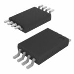 FST3306MTCX
The activity of extra discounts on wholesale prices is in full swing…
Please fill in your contact information and we will send you the latest wholesale price list.





