 ChipApex | Global Electronic Components Supplier
FST3383QSC
Search Product
Search Post
— IC芯片 | 连接器 | 传感器 | 被动器件 —
Search productSearch post
— IC芯片 | 连接器 | 传感器 | 被动器件 —
Consult the customer manager about the wholesale price.
consultation hotline:86-132-6715-2157
email:[email protected]
Contact the product manager for consultation. One-stop consultation is available.
Do you want a lower wholesale price? Please send us your inquiry and we will reply immediately.
The FST3383QSC is a 10-bit low power bus-exchange switch manufactured by onsemi, formerly Fairchild Semiconductor. It provides two sets of high-speed CMOS TTL-compatible bus switches with a typical on-resistance of 5Ω and zero propagation delay. The device operates as a 10-bit bus switch or a 5-bit bus exchanger using the BX signal for nibble swapping. It features ultra-low quiescent supply current (0.2 μA) and zero ground bounce in flow-through mode. Recommended operating conditions specify a supply voltage range of 4.0V to 5.5V and an operating temperature range of -40°C to +85°C.
Verify that the component corresponds to the MQA24 package designation when sourcing the FST3383QSC variant. Confirm the manufacturer lineage from Fairchild Semiconductor to onsemi for accurate documentation access. Ensure the application environment remains within the specified -40°C to +85°C temperature range and 4.0V to 5.5V supply voltage limits to maintain electrical characteristics.
Select this component for designs requiring bidirectional data routing with minimal signal distortion. The integrated bus exchange capability simplifies logic required for byte manipulation compared to discrete multiplexers. Consider the low capacitance and fast enable times for high-frequency applications where timing integrity is critical.
This device belongs to the FST series of bus switches derived from proven CMOS technology. It serves as a bridge between different logic families while maintaining signal integrity. The specific QSC suffix denotes the Quarter Size Outline Package (QSOP), distinguishing it from SOIC or TSSOP variants within the same functional family.
Direct replacements include the FST3383WM (SOIC package) and FST3383MTC (TSSOP package). These share identical electrical specifications and pinouts but differ only in physical package dimensions. Verify mechanical clearance before substituting package types.
When BE is Low and BX is High, the device connects B0-B4 to C0-C4 and D0-D4 to A0-A4, effectively exchanging the nibbles.
The switch contributes no propagation delay other than the RC delay of the on-resistance and load capacitance, which is negligible due to the low resistance value.
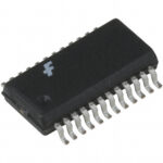 FST3383QSC
The activity of extra discounts on wholesale prices is in full swing…
Please fill in your contact information and we will send you the latest wholesale price list.





