 ChipApex | Global Electronic Components Supplier
HEF4051BP,652
Search Product
Search Post
— IC芯片 | 连接器 | 传感器 | 被动器件 —
Search productSearch post
— IC芯片 | 连接器 | 传感器 | 被动器件 —
Consult the customer manager about the wholesale price.
consultation hotline:86-132-6715-2157
email:[email protected]
Contact the product manager for consultation. One-stop consultation is available.
Do you want a lower wholesale price? Please send us your inquiry and we will reply immediately.
The HEF4051BP,652 is an 8-channel analog multiplexer/demultiplexer manufactured by Nexperia. It operates as a single-pole octal-throw switch with three digital select inputs (S1-S3), eight independent I/Os (Yn), one common I/O (Z), and an active LOW enable input (E). The device supports a supply voltage range of 3.0 V to 15.0 V. Static characteristics include an OFF-state leakage current of up to 1000 nA at 15 V and a maximum ON resistance of 2500 Ω at 5 V. Dynamic performance features propagation delays up to 300 ns and a -3 dB frequency response reaching 70 MHz at 15 V.
Verify the specific suffix '652' against the manufacturer's official ordering information to confirm the package type and tape-and-reel specifications. Confirm that the component meets RoHS compliance requirements for your target market. Ensure the design accounts for the specified ambient temperature operating range of -40 °C to +125 °C during system integration.
Select this component when an 8:1 switching configuration is required within a 3 V to 15 V supply environment. Consider the peak ON resistance limits at your specific operating voltage to ensure signal integrity. Verify that the total harmonic distortion and isolation levels meet the requirements of the intended analog signal path.
This part belongs to the HEF4051B family of 8-channel analog multiplexers produced by Nexperia. The product data sheet revision 14 was released on July 25, 2024. The BP suffix indicates a plastic DIP package variant, distinct from the SO16 or TSSOP16 packages listed in the ordering table.
Direct functional substitutes within the same logic family include other HEF4051 variants such as HEF4051BT or HEF4051BTT, provided the package footprint matches the PCB layout constraints.
The enable input (E) is active LOW. When E is HIGH, all switches are turned off regardless of the state of the select inputs S1, S2, and S3.
The inputs include clamp diodes that allow the use of current-limiting resistors to interface the switch inputs to voltages in excess of the positive supply voltage (VDD).
The total power dissipation (Ptot) is rated at 500 mW over the operating temperature range of -40 °C to +125 °C.
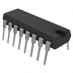 HEF4051BP,652
The activity of extra discounts on wholesale prices is in full swing…
Please fill in your contact information and we will send you the latest wholesale price list.





