 ChipApex | Global Electronic Components Supplier

SEARCH
Search Product
Search Post
— IC芯片 | 连接器 | 传感器 | 被动器件 —
Search productSearch post
— IC芯片 | 连接器 | 传感器 | 被动器件 —
Consult the customer manager about the wholesale price.
consultation hotline:86-132-6715-2157
email:[email protected]
Contact the product manager for consultation. One-stop consultation is available.
Do you want a lower wholesale price? Please send us your inquiry and we will reply immediately.
ICS580M-01I is listed in the Clock Buffers, Drivers range at ChipApex. The manufacturer field lists Renesas Electronics Corporation. Its product description is IC CLK MULTPLX 2:2 270MHZ 16SOIC. Review the specifications below when checking this part for your BOM.
The ICS580M-01I is a glitch-free clock multiplexer manufactured by Renesas Electronics Corporation. It switches between two input clocks (INA and INB) without generating short pulses or glitches on the output. The device operates within a frequency range of 2 MHz to 270 MHz, depending on supply voltage. It features selectable timeout periods for clock detection via the DIV pin, allowing automatic switching when an input clock stops. The component supports split power supplies (VDDI and VDDC) for voltage translation and includes dedicated output enable pins for unused outputs.
Verify RoHS compliance status as non-green parts reached End-of-Life on May 13, 2010. Confirm package availability (SOIC vs TSSOP) and temperature grade (Industrial -40°C to +85°C). Check current distributor stock levels due to potential discontinuation.
Select ICS580M-01I for industrial temperature range (-40°C to +85°C). Ensure VDDI is greater than or equal to VDDC for correct operation. Use OE pins to tri-state unused outputs. Connect decoupling capacitors (0.01µF) to VDDI and VDDC. Consider ICS581-01/02 for zero-delay buffering requirements.
Part of the ICS580 family of glitch-free clock multiplexers. The 'M' suffix indicates commercial temperature range in some variants, but 'I' denotes Industrial grade. Manufactured originally by IDT, now under Renesas Electronics. Available in 16-pin SOIC and TSSOP packages.
ICS581-01 or ICS581-02 offer zero-delay buffering with smooth switching. Verify pin compatibility and electrical specifications before substitution. Check for updated RoHS-compliant versions if environmental regulations require.
It switches between INA and INB inputs controlled by SELB, ensuring no glitches or short pulses appear on the output during transition.
The DIV pin selects the timeout period: Logic 0 provides ~600 ns nominal timeout, while Logic 1 provides ~75 ns nominal timeout.
Yes, VDDI powers the input buffers and can be higher than VDDC, which powers the rest of the chip and sets output amplitude, enabling voltage translation.
Explore related parts through Clock/Timing, Integrated Circuits (ICs), all product categories, ChipApex homepage.
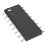 ICS580M-01I
Compare gas sensor technologies, cross-sensitivity and calibration needs. Define the gas, range and environment before choosing a sensing component.
Read More
ICS580M-01I is listed in the Clock Buffers, Drivers range at ChipApex. The manufacturer field lists Renesas Electronics Corporation. Its product description is IC CLK…
Read More
ICS580M-01I is listed in the Clock Buffers, Drivers range at ChipApex. The manufacturer field lists Renesas Electronics Corporation. Its product description is IC CLK…
Read More
Learn why PTC resistance rises with temperature, how it differs from NTC, and which ratings matter for sensing and protection.
Read More
ICS580M-01I is listed in the Clock Buffers, Drivers range at ChipApex. The manufacturer field lists Renesas Electronics Corporation. Its product description is IC CLK…
Read More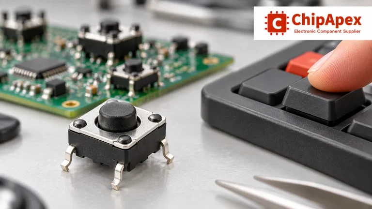
Understand tactile switches, PCB and keyboard differences, four-pin wiring, debounce, force, travel and replacement checks for reliable control inputs.
Read More
ICS580M-01I is listed in the Clock Buffers, Drivers range at ChipApex. The manufacturer field lists Renesas Electronics Corporation. Its product description is IC CLK…
Read More
ICS580M-01I is listed in the Clock Buffers, Drivers range at ChipApex. The manufacturer field lists Renesas Electronics Corporation. Its product description is IC CLK…
Read More
ICS580M-01I is listed in the Clock Buffers, Drivers range at ChipApex. The manufacturer field lists Renesas Electronics Corporation. Its product description is IC CLK…
Read More
ICS580M-01I is listed in the Clock Buffers, Drivers range at ChipApex. The manufacturer field lists Renesas Electronics Corporation. Its product description is IC CLK…
Read MoreICS580M-01I is listed in the Clock Buffers, Drivers range at ChipApex. The manufacturer field lists Renesas Electronics Corporation. Its product description is IC CLK…
Read More
ICS580M-01I is listed in the Clock Buffers, Drivers range at ChipApex. The manufacturer field lists Renesas Electronics Corporation. Its product description is IC CLK…
Read More
The activity of extra discounts on wholesale prices is in full swing…
Please fill in your contact information and we will send you the latest wholesale price list.






