 ChipApex | Global Electronic Components Supplier

SEARCH
Search Product
Search Post
— IC芯片 | 连接器 | 传感器 | 被动器件 —
Search productSearch post
— IC芯片 | 连接器 | 传感器 | 被动器件 —
Consult the customer manager about the wholesale price.
consultation hotline:86-132-6715-2157
email:[email protected]
Contact the product manager for consultation. One-stop consultation is available.
Do you want a lower wholesale price? Please send us your inquiry and we will reply immediately.
ICS83056AGI-01 is listed in the Clock Buffers, Drivers range at ChipApex. The manufacturer field lists Renesas Electronics Corporation. Its product description is IC CLK MULTPX 2:6 250MHZ 20TSSOP. Review the specifications below when checking this part for your BOM.
The ICS83056AGI-01 is a 6-bit, 2:1 single-ended LVCMOS multiplexer from the HiPerClockS family. It features two selectable clock inputs and six independent outputs with a VDDO supply configurable at 3.3V, 2.5V, or 1.8V for voltage translation. The device operates up to 250MHz with typical additive phase jitter of 0.18ps RMS at 155.52MHz (12kHz–20MHz). Propagation delay ranges from 1.5ns to 4.5ns depending on supply conditions. It includes an output enable pin for high-impedance control and functions within a -40°C to 85°C ambient temperature range.
Verify package type upon ordering; the standard suffix 'G' indicates a tube, while 'T' indicates tape and reel packaging. Confirm RoHS compliance requirements by checking for the 'LF' suffix in the part number. Ensure the selected variant matches the required shipping quantity and environmental specifications.
Select based on required output voltage levels (VDDO) and core voltage (VDD) combinations. Verify that the maximum operating frequency of 250MHz meets system timing requirements. Consider the propagation delay variations across different supply modes when designing critical path delays.
This component belongs to the HiPerClockS family of high-performance clock solutions manufactured by IDT (Integrated Device Technology), which was later acquired by Renesas Electronics Corporation. It serves as a specialized timing distribution element for multi-rate data communication systems.
The datasheet lists the 83056AGI-01T, 83056AGI-01LF, and 83056AGI-01LFT as variants differing only in packaging (tape/reel) and lead-free status. No other functional cross-model replacements are documented in the provided source material.
When the OE pin is LOW, all outputs enter a high-impedance state. When HIGH, the outputs are active.
Input skew (tsk(i)) varies by supply mode but is typically 100ps to 145ps under standard test conditions.
Yes, unused CLK inputs can be left floating, though adding a 1kΩ resistor to ground is recommended for additional protection.
Explore related parts through Clock/Timing, Integrated Circuits (ICs), all product categories, ChipApex homepage.
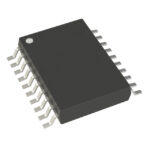 ICS83056AGI-01

ICS83056AGI-01 is listed in the Clock Buffers, Drivers range at ChipApex. The manufacturer field lists Renesas Electronics Corporation. Its product description is IC CLK…
Read More
ICS83056AGI-01 is listed in the Clock Buffers, Drivers range at ChipApex. The manufacturer field lists Renesas Electronics Corporation. Its product description is IC CLK…
Read More
ICS83056AGI-01 is listed in the Clock Buffers, Drivers range at ChipApex. The manufacturer field lists Renesas Electronics Corporation. Its product description is IC CLK…
Read More
Learn how a pressure transducer converts pressure into voltage, current, or digital output, and compare pressure references and key selection specs.
Read More
ICS83056AGI-01 is listed in the Clock Buffers, Drivers range at ChipApex. The manufacturer field lists Renesas Electronics Corporation. Its product description is IC CLK…
Read More
Compare Pt100 and Pt1000 RTDs, two-, three- and four-wire connections, excitation and self-heating. Build an error budget from element to reported temperature.
Read More
ICS83056AGI-01 is listed in the Clock Buffers, Drivers range at ChipApex. The manufacturer field lists Renesas Electronics Corporation. Its product description is IC CLK…
Read More
ICS83056AGI-01 is listed in the Clock Buffers, Drivers range at ChipApex. The manufacturer field lists Renesas Electronics Corporation. Its product description is IC CLK…
Read More
Learn what an IMU measures, how accelerometers and gyroscopes work together, why orientation estimates drift, and what to compare.
Read More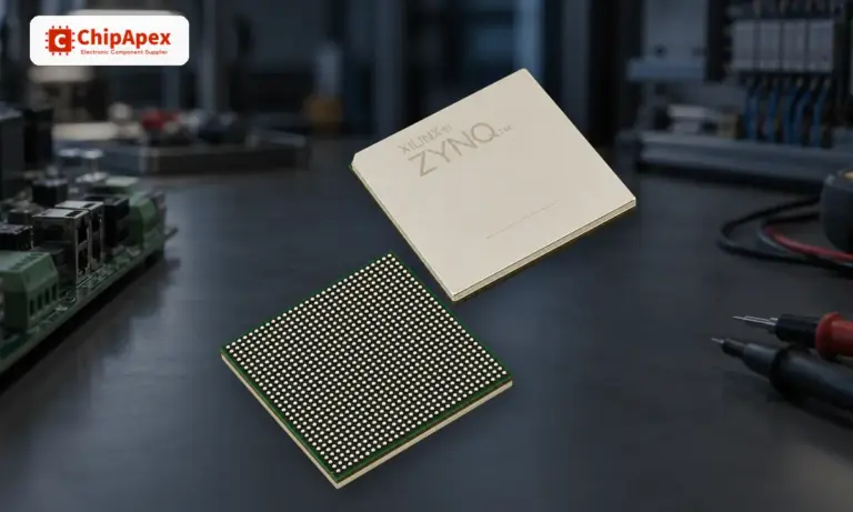
Learn what an integrated circuit is, how ICs work, the main types and the specs to check before choosing a part for your design…
Read More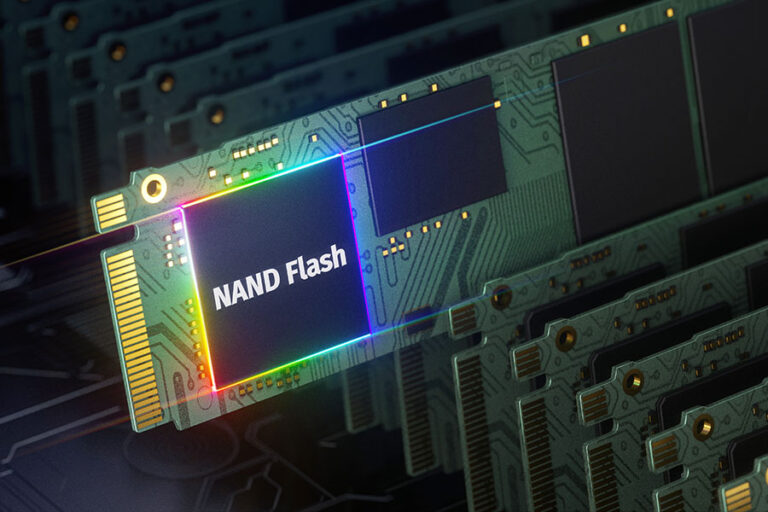
ICS83056AGI-01 is listed in the Clock Buffers, Drivers range at ChipApex. The manufacturer field lists Renesas Electronics Corporation. Its product description is IC CLK…
Read More
ICS83056AGI-01 is listed in the Clock Buffers, Drivers range at ChipApex. The manufacturer field lists Renesas Electronics Corporation. Its product description is IC CLK…
Read More
The activity of extra discounts on wholesale prices is in full swing…
Please fill in your contact information and we will send you the latest wholesale price list.





