 ChipApex | Global Electronic Components Supplier

SEARCH
Search Product
Search Post
— IC芯片 | 连接器 | 传感器 | 被动器件 —
Search productSearch post
— IC芯片 | 连接器 | 传感器 | 被动器件 —
Consult the customer manager about the wholesale price.
consultation hotline:86-132-6715-2157
email:[email protected]
Contact the product manager for consultation. One-stop consultation is available.
Do you want a lower wholesale price? Please send us your inquiry and we will reply immediately.
LAV-AT-E70B-3LFG1156I is listed in the Field Programmable Gate Array range at ChipApex. The manufacturer field lists Lattice Semiconductor Corporation. Its product description is IC FPGA AVANT-E 1156BGA. Review the specifications below when checking this part for your BOM.
The LAV-AT-E70B-3LFG1156I is a Field Programmable Gate Array (FPGA) belonging to the Lattice Avant family, manufactured on a 16nm FinFET process. It features 637,000 logic elements and 35.6 Mbit of embedded memory within an FCBGA-1156 package. The device supports a maximum operating frequency of 2.4 GHz and operates at a supply voltage of 820 mV. It accommodates 554 I/Os and functions within a commercial temperature range of 0°C to +85°C.
Verify the specific suffix '3LFG1156I' against official Lattice documentation to confirm the speed grade, temperature range, and package type match your design requirements. Ensure compatibility with the Radiant software environment for programming and configuration. Check for any recent product change notices regarding availability or pinout modifications before finalizing procurement plans.
Select this component when high logic density and low power consumption are required for mid-range general-purpose applications. Compare the 637k LE count and 35.6 Mbit memory against alternative Avant models to ensure optimal resource utilization. Consider the 16nm process advantages for thermal management and performance efficiency in compact form factors.
This part belongs to the Lattice Avant platform, which targets mid-range FPGA applications requiring high performance and low power. The Avant series utilizes advanced 16nm FinFET technology to deliver improved logic density and energy efficiency compared to previous generations. It is designed for versatile use cases across industrial, automotive, and communications sectors.
Consult Lattice's official cross-reference tools for direct replacements within the Avant family. Verify that any substitute part maintains the same FCBGA-1156 footprint and pinout compatibility. Ensure the alternative device meets or exceeds the 2.4 GHz frequency and 820 mV voltage specifications.
The device is fabricated using a 16nm FinFET process technology.
Yes, the Lattice Avant platform includes hard PCIe IP cores to accelerate system connectivity.
The maximum operating frequency for this device is 2.4 GHz.
Explore related parts through Embedded, Integrated Circuits (ICs), all product categories, ChipApex homepage.

 LAV-AT-E70B-3LFG1156I

LAV-AT-E70B-3LFG1156I is listed in the Field Programmable Gate Array range at ChipApex. The manufacturer field lists Lattice Semiconductor Corporation. Its product description is IC…
Read More
See how a MEMS gyroscope measures angular rate, why its angle estimate drifts, and which range, noise, interface and temperature specs to compare.
Read More
LAV-AT-E70B-3LFG1156I is listed in the Field Programmable Gate Array range at ChipApex. The manufacturer field lists Lattice Semiconductor Corporation. Its product description is IC…
Read More
LAV-AT-E70B-3LFG1156I is listed in the Field Programmable Gate Array range at ChipApex. The manufacturer field lists Lattice Semiconductor Corporation. Its product description is IC…
Read More
Select MOV varistors by continuous voltage, clamping behavior, surge waveform and repetition. Check thermal disconnection, fuse coordination and replacements.
Read More
LAV-AT-E70B-3LFG1156I is listed in the Field Programmable Gate Array range at ChipApex. The manufacturer field lists Lattice Semiconductor Corporation. Its product description is IC…
Read More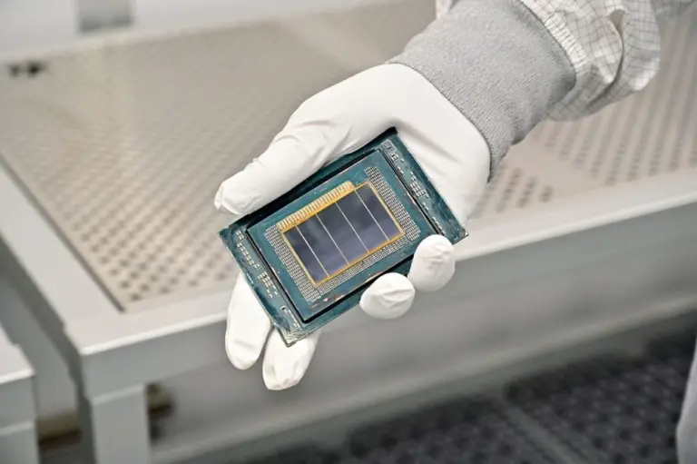
LAV-AT-E70B-3LFG1156I is listed in the Field Programmable Gate Array range at ChipApex. The manufacturer field lists Lattice Semiconductor Corporation. Its product description is IC…
Read More
LAV-AT-E70B-3LFG1156I is listed in the Field Programmable Gate Array range at ChipApex. The manufacturer field lists Lattice Semiconductor Corporation. Its product description is IC…
Read More
Compare thermistors, RTDs, thermocouples and temperature ICs. Learn how range, accuracy, response, interfaces and mounting affect component selection.
Read More
Select a bridge rectifier by reverse voltage, capacitor charging current, startup surge and cooling. Work through a stated DC voltage and ripple example.
Read More
LAV-AT-E70B-3LFG1156I is listed in the Field Programmable Gate Array range at ChipApex. The manufacturer field lists Lattice Semiconductor Corporation. Its product description is IC…
Read More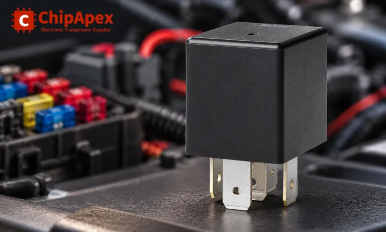
Learn the relay definition, coil and contact operation, NO and NC forms, load ratings and suppression choices. Compare mechanical, reed and solid-state types.
Read More
The activity of extra discounts on wholesale prices is in full swing…
Please fill in your contact information and we will send you the latest wholesale price list.




