ChipApex | Global Electronic Components Supplier

SEARCH
Search Product
Search Post
— IC芯片 | 连接器 | 传感器 | 被动器件 —
Search productSearch post
— IC芯片 | 连接器 | 传感器 | 被动器件 —
Consult the customer manager about the wholesale price.
consultation hotline:86-132-6715-2157
email:[email protected]
Contact the product manager for consultation. One-stop consultation is available.
Do you want a lower wholesale price? Please send us your inquiry and we will reply immediately.
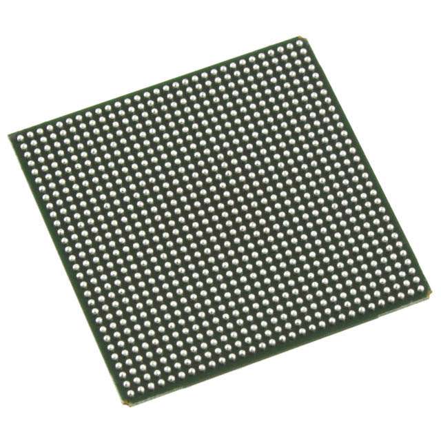
LFE2M100E-6F900I is listed in the Field Programmable Gate Array range at ChipApex. The manufacturer field lists Lattice Semiconductor Corporation. Its product description is IC FPGA 416 I/O 900FBGA. Review the specifications below when checking this part for your BOM.
The LFE2M100E-6F900I is a Field Programmable Gate Array from the Lattice ECP2M family, manufactured by Lattice Semiconductor Corporation. It features 95,000 logic elements and 47,500 Adaptive Logic Modules (ALMs). The device includes 5.18 Mbit of embedded memory, comprising 202 kbit of distributed RAM and 5,308 kbit of Embedded Block RAM (EBR). It supports 416 I/Os and operates within a supply voltage range of 1.14 V to 1.26 V. The component is rated for an industrial temperature range of -40°C to +100°C and utilizes a 900-ball FPBGA package.
Verify the specific suffix '6F900I' against official Lattice documentation, as standard listings often use 'FN900I'. Confirm the speed grade corresponds to the required timing constraints. Ensure the industrial temperature rating matches system requirements. Check for RoHS compliance status in the latest datasheet revision.
Compare this model with the LFE2M100SE variant if low power consumption is critical, noting that the 'E' suffix typically denotes standard performance. Verify pin compatibility with existing PCB layouts using the 900-FPBGA footprint dimensions. Ensure design tools support the specific speed grade for accurate timing closure.
This component belongs to the Lattice ECP2M family, designed for medium-density applications requiring significant logic density and embedded memory. It bridges the gap between lower-density FPGAs and higher-end devices, offering a balance of performance and cost for complex digital designs.
The LFE2M100E-5FN900I is a documented alternative with a different speed grade. Verify functional equivalence regarding I/O counts and memory resources before substitution. No other direct cross-model replacements are confirmed in public sources.
Explore related parts through Embedded, Integrated Circuits (ICs), all product categories, ChipApex homepage.
 LFE2M100E-6F900I
LFE2M100E-6F900I is listed in the Field Programmable Gate Array range at ChipApex. The manufacturer field lists Lattice Semiconductor Corporation. Its product description is IC…
Read More
LFE2M100E-6F900I is listed in the Field Programmable Gate Array range at ChipApex. The manufacturer field lists Lattice Semiconductor Corporation. Its product description is IC…
Read More
LFE2M100E-6F900I is listed in the Field Programmable Gate Array range at ChipApex. The manufacturer field lists Lattice Semiconductor Corporation. Its product description is IC…
Read More
LFE2M100E-6F900I is listed in the Field Programmable Gate Array range at ChipApex. The manufacturer field lists Lattice Semiconductor Corporation. Its product description is IC…
Read More
LFE2M100E-6F900I is listed in the Field Programmable Gate Array range at ChipApex. The manufacturer field lists Lattice Semiconductor Corporation. Its product description is IC…
Read More
See how a MEMS gyroscope measures angular rate, why its angle estimate drifts, and which range, noise, interface and temperature specs to compare.
Read More
LFE2M100E-6F900I is listed in the Field Programmable Gate Array range at ChipApex. The manufacturer field lists Lattice Semiconductor Corporation. Its product description is IC…
Read More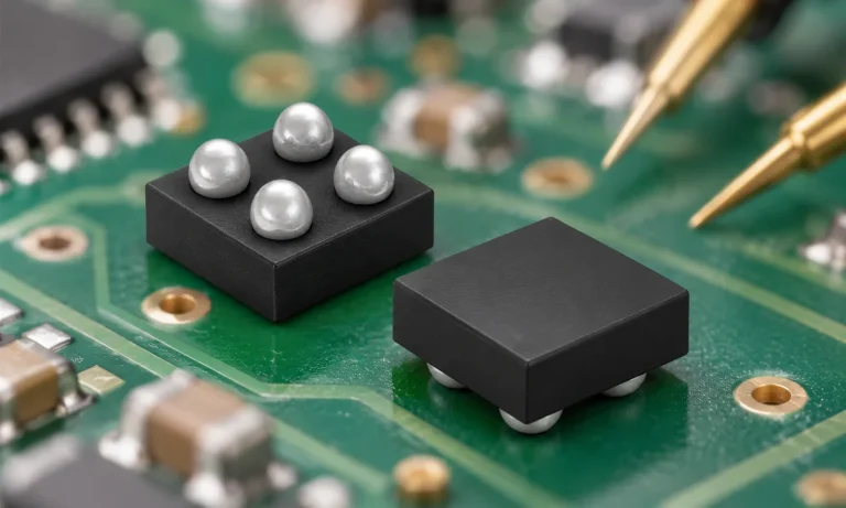
Understand how a comparator switches at a voltage threshold, why hysteresis prevents chatter, and which output and input specs matter.
Read More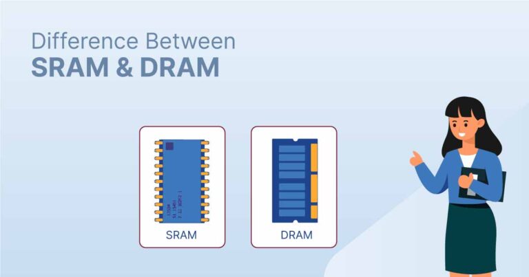
LFE2M100E-6F900I is listed in the Field Programmable Gate Array range at ChipApex. The manufacturer field lists Lattice Semiconductor Corporation. Its product description is IC…
Read More
LFE2M100E-6F900I is listed in the Field Programmable Gate Array range at ChipApex. The manufacturer field lists Lattice Semiconductor Corporation. Its product description is IC…
Read More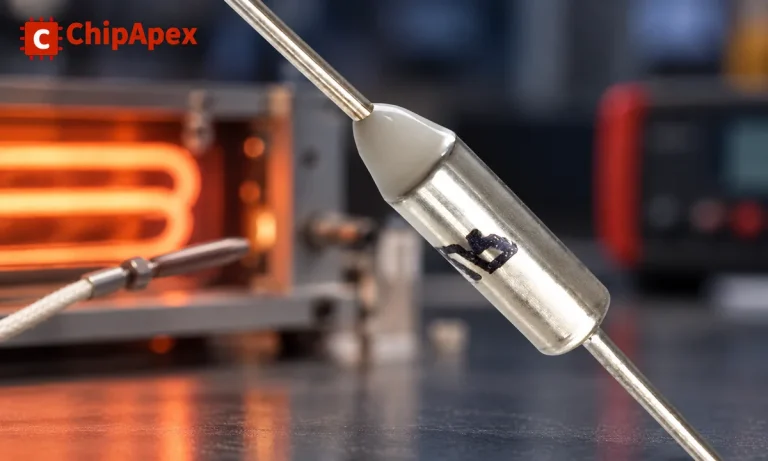
Understand thermal fuse operation, Tf, Th and Tm, electrical ratings and mounting. Check temperature limits and replacement requirements for your design.
Read More
LFE2M100E-6F900I is listed in the Field Programmable Gate Array range at ChipApex. The manufacturer field lists Lattice Semiconductor Corporation. Its product description is IC…
Read More
The activity of extra discounts on wholesale prices is in full swing…
Please fill in your contact information and we will send you the latest wholesale price list.