 ChipApex | Global Electronic Components Supplier

SEARCH
Search Product
Search Post
— IC芯片 | 连接器 | 传感器 | 被动器件 —
Search productSearch post
— IC芯片 | 连接器 | 传感器 | 被动器件 —
Consult the customer manager about the wholesale price.
consultation hotline:86-132-6715-2157
email:[email protected]
Contact the product manager for consultation. One-stop consultation is available.
Do you want a lower wholesale price? Please send us your inquiry and we will reply immediately.
LFECP6E-5QN208C is listed in the Field Programmable Gate Array range at ChipApex. The manufacturer field lists Lattice Semiconductor Corporation. Its product description is IC FPGA 147 I/O 208QFP. Review the specifications below when checking this part for your BOM.
The LFECP6E-5QN208C is a Field Programmable Gate Array from the LatticeECP family, utilizing a 1.2V core voltage and housed in a 208-pin PQFP package with dimensions of 28 x 28 mm. The device provides 6.1K logic elements (LUTs), 97 I/Os, and 25 Kbits of distributed RAM. It includes 92 Kbits of Embedded Block RAM organized into 10 sysMEM blocks and features four sysCLOCK PLLs for clock management.
Verify the specific ordering suffix against the manufacturer's current selection guide to confirm package type and speed grade. Ensure the design tool suite supports the target device architecture. Confirm RoHS compliance status if required by the application environment.
Select this model when a balance of low cost and moderate logic density is required. Compare the 6.1K LUT capacity against system requirements. Verify that the 208-pin PQFP package fits the board layout constraints compared to BGA options.
This component belongs to the LatticeECP/EC family, which is optimized for delivering mainstream FPGA features at a low cost. The family combines an efficient FPGA fabric with high-speed dedicated functions like sysDSP and sysMEM.
Check the LatticeECP/EC Family Selection Guide for devices with similar LUT counts and I/O availability. Consider LFEC6 or LFECP10 variants if higher density is needed, ensuring package compatibility.
Explore related parts through Embedded, Integrated Circuits (ICs), all product categories, ChipApex homepage.
 LFECP6E-5QN208C
LFECP6E-5QN208C is listed in the Field Programmable Gate Array range at ChipApex. The manufacturer field lists Lattice Semiconductor Corporation. Its product description is IC…
Read More
LFECP6E-5QN208C is listed in the Field Programmable Gate Array range at ChipApex. The manufacturer field lists Lattice Semiconductor Corporation. Its product description is IC…
Read More
LFECP6E-5QN208C is listed in the Field Programmable Gate Array range at ChipApex. The manufacturer field lists Lattice Semiconductor Corporation. Its product description is IC…
Read More
LFECP6E-5QN208C is listed in the Field Programmable Gate Array range at ChipApex. The manufacturer field lists Lattice Semiconductor Corporation. Its product description is IC…
Read More
LFECP6E-5QN208C is listed in the Field Programmable Gate Array range at ChipApex. The manufacturer field lists Lattice Semiconductor Corporation. Its product description is IC…
Read More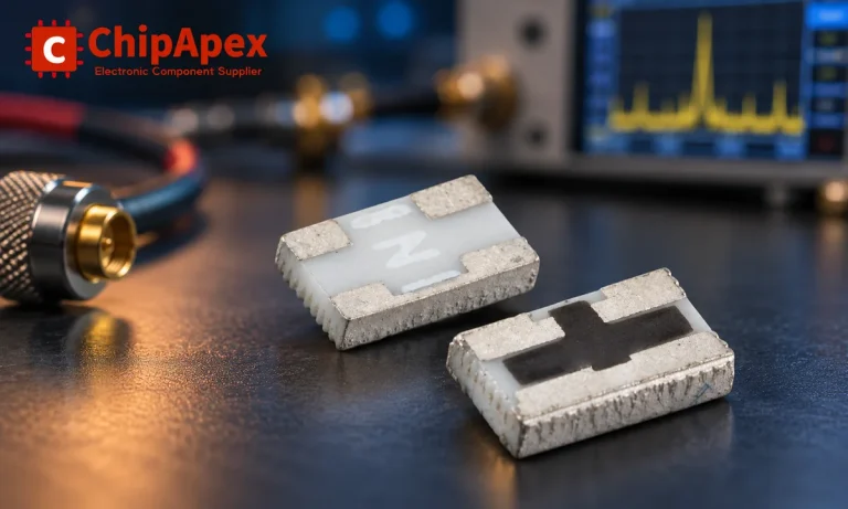
Understand RF attenuator dB values, fixed and programmable types, impedance, power limits and noise tradeoffs before choosing parts for an RF signal path.
Read More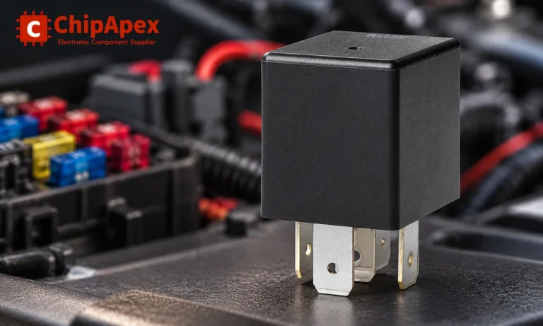
Learn the relay definition, coil and contact operation, NO and NC forms, load ratings and suppression choices. Compare mechanical, reed and solid-state types.
Read More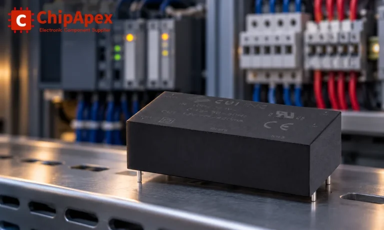
Choose an AC to DC converter by input range, output demand, isolation, efficiency and thermal derating. Compare architectures and check installation needs.
Read More
Find out when a bare shock switch needs a pull resistor, when an MCU internal pull-up is enough, and why sensor modules and piezo…
Read More
LFECP6E-5QN208C is listed in the Field Programmable Gate Array range at ChipApex. The manufacturer field lists Lattice Semiconductor Corporation. Its product description is IC…
Read More
LFECP6E-5QN208C is listed in the Field Programmable Gate Array range at ChipApex. The manufacturer field lists Lattice Semiconductor Corporation. Its product description is IC…
Read More
LFECP6E-5QN208C is listed in the Field Programmable Gate Array range at ChipApex. The manufacturer field lists Lattice Semiconductor Corporation. Its product description is IC…
Read More
The activity of extra discounts on wholesale prices is in full swing…
Please fill in your contact information and we will send you the latest wholesale price list.





