ChipApex | Global Electronic Components Supplier

SEARCH
Search Product
Search Post
— IC芯片 | 连接器 | 传感器 | 被动器件 —
Search productSearch post
— IC芯片 | 连接器 | 传感器 | 被动器件 —
Consult the customer manager about the wholesale price.
consultation hotline:86-132-6715-2157
email:[email protected]
Contact the product manager for consultation. One-stop consultation is available.
Do you want a lower wholesale price? Please send us your inquiry and we will reply immediately.
LTC2051IDD is listed in the Instrumentation, Op Amps, Buffer Amps range at ChipApex. The manufacturer field lists Linear Technology. Its product description is LTC2051 - 2X ZERO-DRIFT OP AMPS. Review the specifications below when checking this part for your BOM.
The LTC2051IDD is a dual zero-drift operational amplifier manufactured by Linear Technology, housed in an 8-lead plastic DFN package measuring 3mm × 3mm. It operates from a single supply voltage ranging from 2.7V to ±5.5V with a typical supply current of 0.75mA per amplifier. The device features a maximum input offset voltage of 3μV and a maximum drift of 30nV/°C. It provides a typical open-loop gain of 140dB, PSRR and CMRR exceeding 130dB, and a gain-bandwidth product of 3MHz. The specified operating temperature range for this part number is –40°C to 85°C.
Verify the specific suffix IDD against manufacturer documentation to confirm the –40°C to 85°C industrial temperature grade and DFN package type. Ensure compatibility with system power supplies within the 2.7V to ±5.5V range. Confirm that the 3mm × 3mm footprint aligns with PCB layout constraints and thermal requirements.
Select this component when ultralow offset voltage and drift are critical for precision signal conditioning. The dual configuration allows cost-effective implementation of differential stages or composite amplifier topologies. Consider the 3MHz bandwidth and 2V/μs slew rate for applications requiring moderate speed alongside high DC accuracy.
The LTC2051 is part of a family of zero-drift operational amplifiers designed for space-constrained applications. It complements the quad-channel LTC2052 and offers performance comparable to larger packages while maintaining a small footprint. The device integrates internal sampling capacitors to eliminate external components for offset correction.
LTC2051CMS8
The device exhibits residue clock feedthrough of less than 1μV RMS input referred at 7.5kHz. Placing a capacitor across the feedback resistor can reduce this effect by limiting closed-loop bandwidth.
Above 70°C, leakage of ESD protection diodes increases input bias currents in the positive direction. Above 85°C, leakage current dominates, causing both input pins to draw current into the device.
Explore related parts through Amplifiers, Linear, Integrated Circuits (ICs), all product categories.
 LTC2051IDD

Choose an AC to DC converter by input range, output demand, isolation, efficiency and thermal derating. Compare architectures and check installation needs.
Read More
LTC2051IDD is listed in the Instrumentation, Op Amps, Buffer Amps range at ChipApex. The manufacturer field lists Linear Technology. Its product description is LTC2051…
Read More
LTC2051IDD is listed in the Instrumentation, Op Amps, Buffer Amps range at ChipApex. The manufacturer field lists Linear Technology. Its product description is LTC2051…
Read More
LTC2051IDD is listed in the Instrumentation, Op Amps, Buffer Amps range at ChipApex. The manufacturer field lists Linear Technology. Its product description is LTC2051…
Read More
LTC2051IDD is listed in the Instrumentation, Op Amps, Buffer Amps range at ChipApex. The manufacturer field lists Linear Technology. Its product description is LTC2051…
Read More
LTC2051IDD is listed in the Instrumentation, Op Amps, Buffer Amps range at ChipApex. The manufacturer field lists Linear Technology. Its product description is LTC2051…
Read More
LTC2051IDD is listed in the Instrumentation, Op Amps, Buffer Amps range at ChipApex. The manufacturer field lists Linear Technology. Its product description is LTC2051…
Read More
LTC2051IDD is listed in the Instrumentation, Op Amps, Buffer Amps range at ChipApex. The manufacturer field lists Linear Technology. Its product description is LTC2051…
Read More
LTC2051IDD is listed in the Instrumentation, Op Amps, Buffer Amps range at ChipApex. The manufacturer field lists Linear Technology. Its product description is LTC2051…
Read More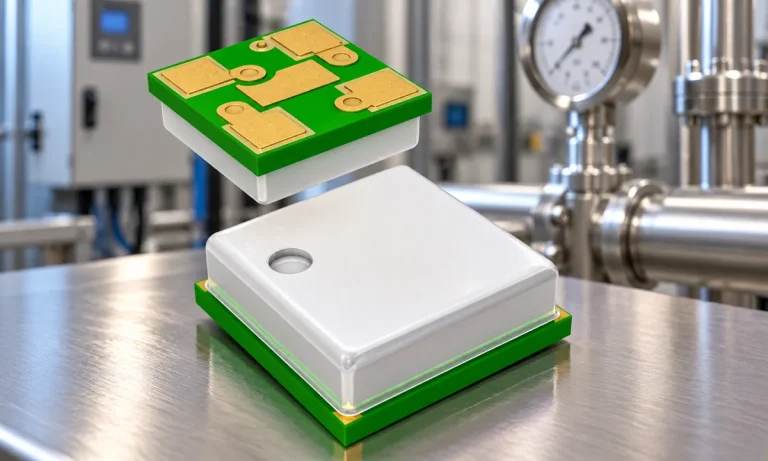
Learn how a pressure transducer converts pressure into voltage, current, or digital output, and compare pressure references and key selection specs.
Read More
LTC2051IDD is listed in the Instrumentation, Op Amps, Buffer Amps range at ChipApex. The manufacturer field lists Linear Technology. Its product description is LTC2051…
Read More
LTC2051IDD is listed in the Instrumentation, Op Amps, Buffer Amps range at ChipApex. The manufacturer field lists Linear Technology. Its product description is LTC2051…
Read More
The activity of extra discounts on wholesale prices is in full swing…
Please fill in your contact information and we will send you the latest wholesale price list.