ChipApex | Global Electronic Components Supplier

SEARCH
Search Product
Search Post
— IC芯片 | 连接器 | 传感器 | 被动器件 —
Search productSearch post
— IC芯片 | 连接器 | 传感器 | 被动器件 —
Consult the customer manager about the wholesale price.
consultation hotline:86-132-6715-2157
email:[email protected]
Contact the product manager for consultation. One-stop consultation is available.
Do you want a lower wholesale price? Please send us your inquiry and we will reply immediately.
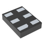
MAX44260AYT+T is listed in the Instrumentation, Op Amps, Buffer Amps range at ChipApex. The manufacturer field lists Analog Devices Inc./Maxim Integrated. Its product description is IC OPAMP GP 1 CIRCUIT 6UTLGA. Review the specifications below when checking this part for your BOM.
The MAX44260AYT+T is a single-channel, low-offset, low-power operational amplifier featuring rail-to-rail input and output capabilities. It operates within a supply voltage range of 1.8V to 5.5V (or 1.7V at 0°C to +70°C) and supports an operating temperature range from -40°C to +125°C. The device incorporates a fast-power-on shutdown mode that reduces quiescent current to less than 1µA with a recovery time under 30µs. Key electrical specifications include a unity-gain bandwidth of 15MHz, a slew rate of 7V/µs, and a maximum input offset voltage of 500µV across the full temperature range. It utilizes a unique input stage architecture with an integrated charge pump to eliminate crossover distortion.
Verify the specific package suffix 'YT' corresponds to the Thin µDFN (Ultra-Thin LGA) configuration when sourcing components. Confirm RoHS compliance status via official manufacturer documentation or authorized distributor declarations prior to procurement. Ensure the ordering part number matches the required pinout and thermal characteristics for the intended PCB layout.
Select this component for designs requiring high precision combined with low power consumption in space-constrained environments. The inclusion of a dedicated shutdown pin makes it suitable for battery-powered systems requiring extended standby modes. Consider the 1mm x 1.5mm footprint when evaluating board real estate against other family members like the SC70 variant.
This device belongs to the MAX44259/MAX44260/MAX44261/MAX44263 family of 1.8V, 15MHz low-offset, low-power, rail-to-rail I/O op amps. While sharing core performance metrics such as bandwidth and noise density, the MAX44260AYT+T is distinguished by its specific 6-pin Thin µDFN packaging and the integration of a shutdown control feature not present in all family variants.
The MAX44260AXT+ serves as a direct functional substitute utilizing the same electrical specifications but housed in a 6-pin SC70 package instead of the Thin µDFN format. Designers must verify mechanical footprint compatibility and thermal dissipation requirements when swapping between these package types.
It employs a unique input stage architecture powered by an integrated, ultra-quiet charge pump that creates an internal voltage rail above VDD. This design eliminates the crossover distortion typically found in standard CMOS input structures.
Upon exiting shutdown mode, the device recovers in under 30µs. It retains its power-up trim settings and does not perform a new self-calibration sequence during this transition.
Explore related parts through Amplifiers, Linear, Integrated Circuits (ICs), all product categories.
 MAX44260AYT+T
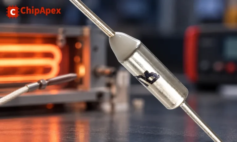
Understand thermal fuse operation, Tf, Th and Tm, electrical ratings and mounting. Check temperature limits and replacement requirements for your design.
Read More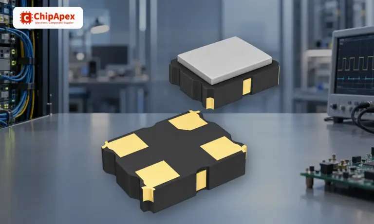
Understand how oscillators generate timing signals, how they differ from crystals, and which frequency, output and stability specs matter when choosing one.
Read More
MAX44260AYT+T is listed in the Instrumentation, Op Amps, Buffer Amps range at ChipApex. The manufacturer field lists Analog Devices Inc./Maxim Integrated. Its product description…
Read More
MAX44260AYT+T is listed in the Instrumentation, Op Amps, Buffer Amps range at ChipApex. The manufacturer field lists Analog Devices Inc./Maxim Integrated. Its product description…
Read More
MAX44260AYT+T is listed in the Instrumentation, Op Amps, Buffer Amps range at ChipApex. The manufacturer field lists Analog Devices Inc./Maxim Integrated. Its product description…
Read More
MAX44260AYT+T is listed in the Instrumentation, Op Amps, Buffer Amps range at ChipApex. The manufacturer field lists Analog Devices Inc./Maxim Integrated. Its product description…
Read More
MAX44260AYT+T is listed in the Instrumentation, Op Amps, Buffer Amps range at ChipApex. The manufacturer field lists Analog Devices Inc./Maxim Integrated. Its product description…
Read More
MAX44260AYT+T is listed in the Instrumentation, Op Amps, Buffer Amps range at ChipApex. The manufacturer field lists Analog Devices Inc./Maxim Integrated. Its product description…
Read More
Learn how rectifiers convert AC to DC, compare half-wave and bridge circuits, and select voltage, current, recovery and thermal ratings for your design.
Read More
MAX44260AYT+T is listed in the Instrumentation, Op Amps, Buffer Amps range at ChipApex. The manufacturer field lists Analog Devices Inc./Maxim Integrated. Its product description…
Read More
MAX44260AYT+T is listed in the Instrumentation, Op Amps, Buffer Amps range at ChipApex. The manufacturer field lists Analog Devices Inc./Maxim Integrated. Its product description…
Read More
MAX44260AYT+T is listed in the Instrumentation, Op Amps, Buffer Amps range at ChipApex. The manufacturer field lists Analog Devices Inc./Maxim Integrated. Its product description…
Read More
The activity of extra discounts on wholesale prices is in full swing…
Please fill in your contact information and we will send you the latest wholesale price list.