 ChipApex | Global Electronic Components Supplier

SEARCH
Search Product
Search Post
— IC芯片 | 连接器 | 传感器 | 被动器件 —
Search productSearch post
— IC芯片 | 连接器 | 传感器 | 被动器件 —
Consult the customer manager about the wholesale price.
consultation hotline:86-132-6715-2157
email:[email protected]
Contact the product manager for consultation. One-stop consultation is available.
Do you want a lower wholesale price? Please send us your inquiry and we will reply immediately.
MC100E310FNR2G is listed in the Clock Buffers, Drivers range at ChipApex. The manufacturer field lists onsemi. Its product description is IC CLK BUFFER 2:8 900MHZ 28PLCC. Review the specifications below when checking this part for your BOM.
The MC100E310FNR2G is a low voltage, low skew differential ECL fanout buffer designed for clock distribution. It features two selectable differential clock inputs (CLKa/CLKb) and provides eight differential outputs with a 2:8 ratio. The device operates in PECL mode with VCC = 4.2 V to 5.7 V or NECL mode with VEE = -4.2 V to -5.7 V. Maximum toggle frequency is 900 MHz at 25°C. Typical within-device skew is 50 ps, and part-to-part skew is 200 ps. It includes an internal reference voltage output (VBB), input pulldown resistors, and ESD protection exceeding 2 kV HBM. The component is housed in a 28-lead PLCC package.
Verify that the specific order suffix 'R2G' corresponds to the Tape & Reel packaging format containing 500 units per reel. Confirm RoHS compliance status as the datasheet indicates Pb-Free and Halogen Free characteristics for this marking. Ensure power supply connections for all VCC, VCCO, and VEE pins are externally connected to guarantee proper operation.
Select this component when dual independent clock sources are required for redundancy or testing within a single buffer stage. The 2:8 fanout ratio suits designs needing one signal distributed to eight destinations. Consider the 50 ps typical skew for tight timing budgets. Verify compatibility with PECL (+5V) or NECL (-5V) supply configurations based on system architecture.
The MC100E310 belongs to the onsemi 100E Series, which contains temperature compensation. This series is part of the ECLinPS family of high-performance ECL devices. The FNR2G suffix denotes the 28-lead PLCC package variant supplied in tape and reel format, distinct from the tube-packaged FNG version.
Public confirmed substitute part numbers are not provided in the source material. Designers should consult application notes AN1406/D and AND8003/D for interfacing guidelines and moisture sensitivity handling if replacing existing inventory.
The CLK_SEL pin determines the active input. A logic low selects CLKa, while a logic high selects CLKb.
VBB provides an internally generated reference voltage. It can be used to bias unused differential inputs for single-ended operation or to rebias AC-coupled inputs. It must be decoupled with a 0.01 µF capacitor if used.
The maximum toggle frequency (fMAX) is 900 MHz at 25°C, with a minimum guaranteed specification of 700 MHz across the operating temperature range.
Explore related parts through Clock/Timing, Integrated Circuits (ICs), all product categories, ChipApex homepage.
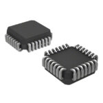 MC100E310FNR2G

MC100E310FNR2G is listed in the Clock Buffers, Drivers range at ChipApex. The manufacturer field lists onsemi. Its product description is IC CLK BUFFER 2:8…
Read More
MC100E310FNR2G is listed in the Clock Buffers, Drivers range at ChipApex. The manufacturer field lists onsemi. Its product description is IC CLK BUFFER 2:8…
Read More
MC100E310FNR2G is listed in the Clock Buffers, Drivers range at ChipApex. The manufacturer field lists onsemi. Its product description is IC CLK BUFFER 2:8…
Read More
Compare RC, crystal and MEMS oscillator circuits. Check ppm, jitter, load capacitance, startup margin and output compatibility before choosing a clock source.
Read More
MC100E310FNR2G is listed in the Clock Buffers, Drivers range at ChipApex. The manufacturer field lists onsemi. Its product description is IC CLK BUFFER 2:8…
Read More
MC100E310FNR2G is listed in the Clock Buffers, Drivers range at ChipApex. The manufacturer field lists onsemi. Its product description is IC CLK BUFFER 2:8…
Read More
Select MOV varistors by continuous voltage, clamping behavior, surge waveform and repetition. Check thermal disconnection, fuse coordination and replacements.
Read More
MC100E310FNR2G is listed in the Clock Buffers, Drivers range at ChipApex. The manufacturer field lists onsemi. Its product description is IC CLK BUFFER 2:8…
Read More
Understand how a comparator switches at a voltage threshold, why hysteresis prevents chatter, and which output and input specs matter.
Read More
Choose an AC to DC converter by input range, output demand, isolation, efficiency and thermal derating. Compare architectures and check installation needs.
Read More
MC100E310FNR2G is listed in the Clock Buffers, Drivers range at ChipApex. The manufacturer field lists onsemi. Its product description is IC CLK BUFFER 2:8…
Read More
Select a bridge rectifier by reverse voltage, capacitor charging current, startup surge and cooling. Work through a stated DC voltage and ripple example.
Read More
The activity of extra discounts on wholesale prices is in full swing…
Please fill in your contact information and we will send you the latest wholesale price list.





