 ChipApex | Global Electronic Components Supplier

SEARCH
Search Product
Search Post
— IC芯片 | 连接器 | 传感器 | 被动器件 —
Search productSearch post
— IC芯片 | 连接器 | 传感器 | 被动器件 —
Consult the customer manager about the wholesale price.
consultation hotline:86-132-6715-2157
email:[email protected]
Contact the product manager for consultation. One-stop consultation is available.
Do you want a lower wholesale price? Please send us your inquiry and we will reply immediately.
MC100EP142FAG is listed in the Shift Registers range at ChipApex. The manufacturer field lists onsemi. Its product description is IC REGISTER SHFT 9BIT ECL 32LQFP. Review the specifications below when checking this part for your BOM.
The MC100EP142FAG is a 9-bit shift register from the onsemi 100E series, designed for byte-parity applications. It supports serial/parallel data input and serial/parallel output with unidirectional shifting capability. The device operates in PECL mode (VCC = 3.0 V to 5.5 V, VEE = 0 V) or NECL mode (VCC = 0 V, VEE = -3.0 V to -5.5 V). It features dual differential clocks (CLK0, CLK1), asynchronous master reset, and temperature compensation. The component is housed in a lead-free LQFP-32 package.
Verify the specific ordering suffix 'FA' corresponds to the LQFP-32 package configuration as defined in the manufacturer's documentation. Confirm RoHS compliance status and Pb-Free designation requirements for the target assembly process. Ensure voltage supply rails match the specified PECL or NECL operating ranges to prevent device malfunction.
Select this component when a 9-bit ECL shift register with dual-clock support is required for byte-oriented data handling. Consider the LQFP-32 package constraints for thermal management and PCB layout. Evaluate the need for asynchronous reset and unidirectional shifting against alternative logic families if lower power consumption is critical.
This part belongs to the MC10EP/100EP142 family of high-speed ECL shift registers. The '100' prefix indicates the 100E series variant, which includes temperature compensation compared to the standard 10E series. It is functionally compatible with other devices in the ECLinPS portfolio designed for similar high-frequency logic applications.
MC100EP142MNG is a documented equivalent offering the same logical function in a QFN-32 package.
The SEL pin switches between SHIFT and LOAD modes. When SEL is low, parallel data inputs are loaded into the registers. When SEL is high, the device shifts data serially from Bit 0 to Bit 8 on the positive clock edge.
A HIGH signal on the MR pin asynchronously resets all nine registers to zero. This action overrides the CLK0 and CLK1 inputs immediately.
No, the QT0:8 outputs do not need to be terminated for the shift operation to function correctly. However, leaving unused Q outputs unterminated helps minimize power consumption.
Explore related parts through Logic, Integrated Circuits (ICs), all product categories, ChipApex homepage.
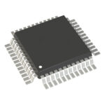 MC100EP142FAG

MC100EP142FAG is listed in the Shift Registers range at ChipApex. The manufacturer field lists onsemi. Its product description is IC REGISTER SHFT 9BIT ECL…
Read More
MC100EP142FAG is listed in the Shift Registers range at ChipApex. The manufacturer field lists onsemi. Its product description is IC REGISTER SHFT 9BIT ECL…
Read More
MC100EP142FAG is listed in the Shift Registers range at ChipApex. The manufacturer field lists onsemi. Its product description is IC REGISTER SHFT 9BIT ECL…
Read More
Understand tactile switches, PCB and keyboard differences, four-pin wiring, debounce, force, travel and replacement checks for reliable control inputs.
Read More
Learn why PTC resistance rises with temperature, how it differs from NTC, and which ratings matter for sensing and protection.
Read More
MC100EP142FAG is listed in the Shift Registers range at ChipApex. The manufacturer field lists onsemi. Its product description is IC REGISTER SHFT 9BIT ECL…
Read More
MC100EP142FAG is listed in the Shift Registers range at ChipApex. The manufacturer field lists onsemi. Its product description is IC REGISTER SHFT 9BIT ECL…
Read More
Learn how a pressure transducer converts pressure into voltage, current, or digital output, and compare pressure references and key selection specs.
Read More
MC100EP142FAG is listed in the Shift Registers range at ChipApex. The manufacturer field lists onsemi. Its product description is IC REGISTER SHFT 9BIT ECL…
Read More
MC100EP142FAG is listed in the Shift Registers range at ChipApex. The manufacturer field lists onsemi. Its product description is IC REGISTER SHFT 9BIT ECL…
Read More
MC100EP142FAG is listed in the Shift Registers range at ChipApex. The manufacturer field lists onsemi. Its product description is IC REGISTER SHFT 9BIT ECL…
Read More
MC100EP142FAG is listed in the Shift Registers range at ChipApex. The manufacturer field lists onsemi. Its product description is IC REGISTER SHFT 9BIT ECL…
Read More
The activity of extra discounts on wholesale prices is in full swing…
Please fill in your contact information and we will send you the latest wholesale price list.






