 ChipApex | Global Electronic Components Supplier

SEARCH
Search Product
Search Post
— IC芯片 | 连接器 | 传感器 | 被动器件 —
Search productSearch post
— IC芯片 | 连接器 | 传感器 | 被动器件 —
Consult the customer manager about the wholesale price.
consultation hotline:86-132-6715-2157
email:[email protected]
Contact the product manager for consultation. One-stop consultation is available.
Do you want a lower wholesale price? Please send us your inquiry and we will reply immediately.
MC100ES8111FA is listed in the Clock Buffers, Drivers range at ChipApex. The manufacturer field lists NXP USA Inc.. Its product description is IC CLK BUFFER 2:10 625MHZ 32LQFP. Review the specifications below when checking this part for your BOM.
The MC100ES8111 is a low-voltage, bipolar monolithic differential clock fanout buffer designed for high-performance clock distribution in computing, networking, and telecommunications systems. Utilizing SiGe technology, it provides a 1:10 split of precisely aligned differential clock signals with very low skew. The device accepts HSTL-compatible inputs on the CLK0 pair and PECL-compatible inputs on the CLK1 pair, distributing the selected signal to ten identical HSTL-compatible differential outputs. It operates at frequencies up to 625 MHz using a 3.3 V core supply and a 1.5 V or 1.8 V output supply.
Verify that the package matches the standard 32-lead LQFP (Case 873A-03). Confirm the specific ordering suffix corresponds to the required tape and reel or tube configuration, as these affect physical packaging but not electrical function. Ensure the component meets industrial temperature range requirements if operating outside standard commercial limits.
Select this component when low skew and precise alignment are critical for distributing a single clock source to multiple destinations. Ensure the design accommodates the dual power supply requirement: 3.3 V for the core and either 1.5 V or 1.8 V for the HSTL outputs. Verify that the application can support the necessary 50 Ω DC termination to ground for all active differential output pairs to maintain specified timing characteristics.
The MC100ES8111 belongs to the Advanced Clock Drivers family from Freescale Semiconductor (now NXP USA Inc.). It is specifically engineered for demanding clock distribution architectures where signal integrity and timing precision are paramount. The device leverages SiGe technology to achieve superior digital signal characteristics compared to standard CMOS alternatives.
Public confirmed substitute part numbers are not available in the provided documentation. When evaluating potential replacements, ensure the alternative supports 1:10 differential fanout, maintains similar skew specifications (under 80 ps), and is compatible with both HSTL and PECL input standards.
To maintain tight skew specifications, both outputs of any differential pair must be terminated identically with 50 Ω resistors to GND, even if only one side of the pair is used. If an entire bank of outputs is unused, it is recommended to leave them open and unterminated.
The OE (Output Enable) pin controls the state of the outputs. It is internally synchronized to the input reference clock to prevent the generation of output runt pulses. Outputs are disabled in the logic low state without changing output impedance.
No, the device does not support output termination to VTT = VX = 0.75 V. It requires a 50 Ω DC termination to GND (0 V) for correct AC and DC operation.
Explore related parts through Clock/Timing, Integrated Circuits (ICs), all product categories, ChipApex homepage.
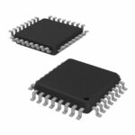 MC100ES8111FA
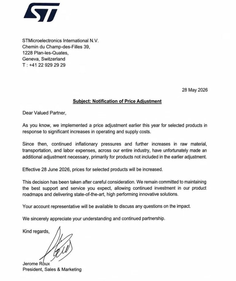
MC100ES8111FA is listed in the Clock Buffers, Drivers range at ChipApex. The manufacturer field lists NXP USA Inc.. Its product description is IC CLK…
Read More
MC100ES8111FA is listed in the Clock Buffers, Drivers range at ChipApex. The manufacturer field lists NXP USA Inc.. Its product description is IC CLK…
Read More
Select MOV varistors by continuous voltage, clamping behavior, surge waveform and repetition. Check thermal disconnection, fuse coordination and replacements.
Read More
MC100ES8111FA is listed in the Clock Buffers, Drivers range at ChipApex. The manufacturer field lists NXP USA Inc.. Its product description is IC CLK…
Read More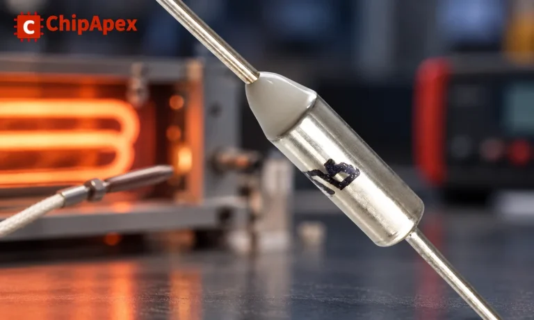
Understand thermal fuse operation, Tf, Th and Tm, electrical ratings and mounting. Check temperature limits and replacement requirements for your design.
Read More
MC100ES8111FA is listed in the Clock Buffers, Drivers range at ChipApex. The manufacturer field lists NXP USA Inc.. Its product description is IC CLK…
Read More
MC100ES8111FA is listed in the Clock Buffers, Drivers range at ChipApex. The manufacturer field lists NXP USA Inc.. Its product description is IC CLK…
Read More
MC100ES8111FA is listed in the Clock Buffers, Drivers range at ChipApex. The manufacturer field lists NXP USA Inc.. Its product description is IC CLK…
Read More
MC100ES8111FA is listed in the Clock Buffers, Drivers range at ChipApex. The manufacturer field lists NXP USA Inc.. Its product description is IC CLK…
Read More
MC100ES8111FA is listed in the Clock Buffers, Drivers range at ChipApex. The manufacturer field lists NXP USA Inc.. Its product description is IC CLK…
Read More
MC100ES8111FA is listed in the Clock Buffers, Drivers range at ChipApex. The manufacturer field lists NXP USA Inc.. Its product description is IC CLK…
Read More
MC100ES8111FA is listed in the Clock Buffers, Drivers range at ChipApex. The manufacturer field lists NXP USA Inc.. Its product description is IC CLK…
Read More
The activity of extra discounts on wholesale prices is in full swing…
Please fill in your contact information and we will send you the latest wholesale price list.





