 ChipApex | Global Electronic Components Supplier

SEARCH
Search Product
Search Post
— IC芯片 | 连接器 | 传感器 | 被动器件 —
Search productSearch post
— IC芯片 | 连接器 | 传感器 | 被动器件 —
Consult the customer manager about the wholesale price.
consultation hotline:86-132-6715-2157
email:[email protected]
Contact the product manager for consultation. One-stop consultation is available.
Do you want a lower wholesale price? Please send us your inquiry and we will reply immediately.
MC10E211FN is listed in the Clock Buffers, Drivers range at ChipApex. The manufacturer field lists onsemi. Its product description is IC CLK BUFFER 2:6 700MHZ 28PLCC. Review the specifications below when checking this part for your BOM.
The MC10E211FN is a low skew 1:6 fanout differential clock distribution chip from onsemi. It features multiplexed clock inputs for distributing high-speed system clocks and lower-speed scan/test clocks. The device supports PECL mode (VCC = 4.2 V to 5.7 V, VEE = 0 V) and NECL mode (VCC = 0 V, VEE = −4.2 V to −5.7 V). Key electrical parameters include a maximum toggle frequency of 700 MHz, typical propagation delay of 745 ps (CLK to Q diff), and guaranteed part-to-part skew of 50 ps. It operates within a temperature range of 0°C to +85°C and is housed in a PLCC-28 package.
Verify the ordering suffix to confirm packaging type. The 'FN' suffix indicates a PLCC-28 tube containing 37 units. The 'FNR2' suffix denotes a tape and reel containing 500 units. Confirm RoHS compliance requirements, as 'G' suffixes indicate lead-free packages. Ensure power supply connections for all VCC, VCCO, and VEE pins are established to guarantee proper operation.
Select the MC10E211FN when a 1:6 fanout with tight skew specifications is required. Use this device instead of the E111 if lower fanout and higher bandwidth output transistors are needed for faster edge rates. Choose the 10 series (MC10E...) for standard operation or the 100 series (MC100E...) if temperature compensation is necessary. Ensure the application can accommodate the required termination schemes for unused outputs to maintain skew performance.
The MC10E211 is part of the ECLinPS family, designed specifically for clock distribution applications. It complements the MC10E111 by providing a secondary level of distribution with individual enable capabilities. The device is characterized for operation up to 700 MHz and is intended for use in conjunction with other ECL logic devices to build complex clock networks.
Public confirmed substitute part numbers are not available in the provided documentation. Designers should verify compatibility with existing clock tree architectures when considering alternative components.
All input pins have internal pulldown resistors. If differential CLK inputs are left open, the gate current source transistor may saturate, leading to undefined outputs. It is recommended to select the SCLK input if the differential CLK inputs are allowed to float.
To minimize noise and maintain skew performance, unused output pairs (true and complement) should be terminated in pairs. Leaving them unterminated can influence propagation delay on adjacent pins by 15 ps to 20 ps.
Yes, but it requires connecting the unused differential input to the VBB pin as a switching reference. For AC-coupled inputs, the dependence on the VBB centering is removed, allowing the use of differential AC specification limits.
Explore related parts through Clock/Timing, Integrated Circuits (ICs), all product categories, ChipApex homepage.
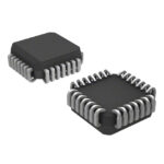 MC10E211FN

MC10E211FN is listed in the Clock Buffers, Drivers range at ChipApex. The manufacturer field lists onsemi. Its product description is IC CLK BUFFER 2:6…
Read More
MC10E211FN is listed in the Clock Buffers, Drivers range at ChipApex. The manufacturer field lists onsemi. Its product description is IC CLK BUFFER 2:6…
Read More
MC10E211FN is listed in the Clock Buffers, Drivers range at ChipApex. The manufacturer field lists onsemi. Its product description is IC CLK BUFFER 2:6…
Read More
MC10E211FN is listed in the Clock Buffers, Drivers range at ChipApex. The manufacturer field lists onsemi. Its product description is IC CLK BUFFER 2:6…
Read More
MC10E211FN is listed in the Clock Buffers, Drivers range at ChipApex. The manufacturer field lists onsemi. Its product description is IC CLK BUFFER 2:6…
Read More
MC10E211FN is listed in the Clock Buffers, Drivers range at ChipApex. The manufacturer field lists onsemi. Its product description is IC CLK BUFFER 2:6…
Read More
MC10E211FN is listed in the Clock Buffers, Drivers range at ChipApex. The manufacturer field lists onsemi. Its product description is IC CLK BUFFER 2:6…
Read More
MC10E211FN is listed in the Clock Buffers, Drivers range at ChipApex. The manufacturer field lists onsemi. Its product description is IC CLK BUFFER 2:6…
Read More
MC10E211FN is listed in the Clock Buffers, Drivers range at ChipApex. The manufacturer field lists onsemi. Its product description is IC CLK BUFFER 2:6…
Read More
MC10E211FN is listed in the Clock Buffers, Drivers range at ChipApex. The manufacturer field lists onsemi. Its product description is IC CLK BUFFER 2:6…
Read More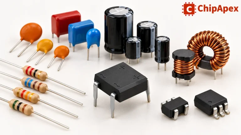
Explore electronic component types, functions, packages and datasheets. Learn selection, replacement and BOM checks before ordering parts for your PCB.
Read More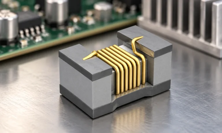
See when an inductor behaves linearly, how DC bias and saturation reduce inductance, and which current and temperature curves to check.
Read More
The activity of extra discounts on wholesale prices is in full swing…
Please fill in your contact information and we will send you the latest wholesale price list.





