 ChipApex | Global Electronic Components Supplier

SEARCH
Search Product
Search Post
— IC芯片 | 连接器 | 传感器 | 被动器件 —
Search productSearch post
— IC芯片 | 连接器 | 传感器 | 被动器件 —
Consult the customer manager about the wholesale price.
consultation hotline:86-132-6715-2157
email:[email protected]
Contact the product manager for consultation. One-stop consultation is available.
Do you want a lower wholesale price? Please send us your inquiry and we will reply immediately.
MC14094BFELG is listed in the Shift Registers range at ChipApex. The manufacturer field lists onsemi. Its product description is IC SHIFT REGISTER 8STG 16SOEIAJ. Review the specifications below when checking this part for your BOM.
The MC14094BFELG is an 8-stage shift/store register with three-state outputs manufactured by onsemi. It integrates an 8-stage shift register, a data latch for each stage, and three-state buffers controlled by an Output Enable signal. Data shifts on the positive clock transition, while latching occurs on the negative strobe transition. The device operates within a DC supply voltage range of -0.5 V to +18.0 V and supports an ambient temperature range of -55 °C to +125 °C. It is housed in a 16-SOEIAJ package and supplied in tape and reel quantities of 2000 units.
Verify the specific ordering suffix 'F' corresponds to the SOEIAJ-16 package configuration as defined in the manufacturer's documentation. Confirm that the procurement channel provides the standard 2000-unit tape and reel packaging format associated with this suffix. Ensure compliance with RoHS standards and lead-free requirements specified for this component variant.
Select this component when an 8-bit shift register with parallel storage and tri-state control is required. It is suitable for applications needing dual serial outputs for different cascade speeds. Verify that the operating voltage and temperature ranges align with system constraints. Consider the SOEIAJ-16 package dimensions for PCB layout compatibility.
This part belongs to the MC14094B family of CMOS logic devices. It serves as a functional equivalent to the industry-standard CD4094B. The device is designed for general-purpose digital logic applications requiring reliable data shifting and storage capabilities within standard CMOS voltage and temperature specifications.
MC14094BDG
Data from the shift register stages is latched onto the parallel outputs upon the negative transition of the strobe input. The data propagates through the latch while the strobe signal remains high.
The QS output transfers data from the seventh stage during the positive clock transition, intended for high-speed cascading. The Q'S output shifts data during the following negative clock transition, designed for low-speed cascading.
Explore related parts through Logic, Integrated Circuits (ICs), all product categories, ChipApex homepage.
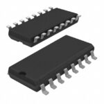 MC14094BFELG

MC14094BFELG is listed in the Shift Registers range at ChipApex. The manufacturer field lists onsemi. Its product description is IC SHIFT REGISTER 8STG 16SOEIAJ.…
Read More
MC14094BFELG is listed in the Shift Registers range at ChipApex. The manufacturer field lists onsemi. Its product description is IC SHIFT REGISTER 8STG 16SOEIAJ.…
Read More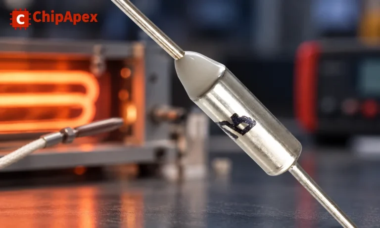
Understand thermal fuse operation, Tf, Th and Tm, electrical ratings and mounting. Check temperature limits and replacement requirements for your design.
Read More
Learn why PTC resistance rises with temperature, how it differs from NTC, and which ratings matter for sensing and protection.
Read More
MC14094BFELG is listed in the Shift Registers range at ChipApex. The manufacturer field lists onsemi. Its product description is IC SHIFT REGISTER 8STG 16SOEIAJ.…
Read More
Choose a DIP switch by contact type, coded positions, footprint and signal ratings. Check logic polarity, assembly conditions and PCB configuration behavior.
Read More
MC14094BFELG is listed in the Shift Registers range at ChipApex. The manufacturer field lists onsemi. Its product description is IC SHIFT REGISTER 8STG 16SOEIAJ.…
Read More
MC14094BFELG is listed in the Shift Registers range at ChipApex. The manufacturer field lists onsemi. Its product description is IC SHIFT REGISTER 8STG 16SOEIAJ.…
Read More
MC14094BFELG is listed in the Shift Registers range at ChipApex. The manufacturer field lists onsemi. Its product description is IC SHIFT REGISTER 8STG 16SOEIAJ.…
Read More
MC14094BFELG is listed in the Shift Registers range at ChipApex. The manufacturer field lists onsemi. Its product description is IC SHIFT REGISTER 8STG 16SOEIAJ.…
Read More
MC14094BFELG is listed in the Shift Registers range at ChipApex. The manufacturer field lists onsemi. Its product description is IC SHIFT REGISTER 8STG 16SOEIAJ.…
Read More
MC14094BFELG is listed in the Shift Registers range at ChipApex. The manufacturer field lists onsemi. Its product description is IC SHIFT REGISTER 8STG 16SOEIAJ.…
Read More
The activity of extra discounts on wholesale prices is in full swing…
Please fill in your contact information and we will send you the latest wholesale price list.






