 ChipApex | Global Electronic Components Supplier

SEARCH
Search Product
Search Post
— IC芯片 | 连接器 | 传感器 | 被动器件 —
Search productSearch post
— IC芯片 | 连接器 | 传感器 | 被动器件 —
Consult the customer manager about the wholesale price.
consultation hotline:86-132-6715-2157
email:[email protected]
Contact the product manager for consultation. One-stop consultation is available.
Do you want a lower wholesale price? Please send us your inquiry and we will reply immediately.
MX25L2026EM1I-12G is listed in the Memory IC range at ChipApex. The manufacturer field lists Macronix. Its product description is IC FLASH 2MBIT SPI 86MHZ 8SOP. Review the specifications below when checking this part for your BOM.
The MX25L2026EM1I-12G is a 2-Mbit CMOS Serial Flash memory device manufactured by Macronix. It features a Serial Peripheral Interface (SPI) compatible with Mode 0 and Mode 3, supporting a maximum serial clock frequency of 86 MHz for standard read operations and 80 MHz in Dual Output mode. The device operates on a single power supply ranging from 2.7 V to 3.6 V. It offers a memory organization of 2,097,152 x 1 bit or 1,048,576 x 2 bits, structured into 64 equal sectors of 4 Kbytes each and 4 equal blocks of 64 Kbytes each. The component is housed in an 8-pin SOP package.
Verify the specific suffix EM1I-12G against the manufacturer's current ordering guide to confirm package type and temperature range. Ensure compatibility with system voltage levels within the 2.7V to 3.6V operating window. Check for RoHS compliance requirements if applicable to your manufacturing process. Confirm lead times as availability may vary by distributor.
Select this component when a small capacity NOR flash with SPI interface is required for code storage. It is suitable for applications needing moderate speed access up to 86 MHz. Consider the 8-pin SOP package constraints for PCB layout. Evaluate the need for dual output mode if higher read speeds are necessary compared to standard SPI.
This part belongs to the MX25L series of 3V Serial Flash memories from Macronix. The series is designed for general-purpose non-volatile storage with low power consumption. It shares common command sets and interface protocols with other members of the MX25L family, facilitating design reuse across different memory densities.
MX25V4006EM1I-13G
Standard Read uses one I/O pin (SO) for data output at up to 86 MHz. Dual Output Read uses both SI and SO pins (SIO0 and SIO1) for data output, allowing faster transfer rates at a maximum clock frequency of 80 MHz.
The Hold feature allows the user to pause serial communication without deasserting Chip Select (CS#). It is activated by pulling the HOLD# pin low while SCLK is low. Data output goes high-impedance during hold, and communication resumes when HOLD# goes high.
Explore related parts through Memory, Integrated Circuits (ICs), all product categories, ChipApex homepage.
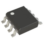 MX25L2026EM1I-12G
See when an inductor behaves linearly, how DC bias and saturation reduce inductance, and which current and temperature curves to check.
Read More
Learn how a diode conducts, how to identify anode and cathode, and when to choose rectifier, TVS, Zener or photodiode types for a circuit.
Read More
Understand thermal fuse operation, Tf, Th and Tm, electrical ratings and mounting. Check temperature limits and replacement requirements for your design.
Read More
MX25L2026EM1I-12G is listed in the Memory IC range at ChipApex. The manufacturer field lists Macronix. Its product description is IC FLASH 2MBIT SPI 86MHZ…
Read More
MX25L2026EM1I-12G is listed in the Memory IC range at ChipApex. The manufacturer field lists Macronix. Its product description is IC FLASH 2MBIT SPI 86MHZ…
Read More
MX25L2026EM1I-12G is listed in the Memory IC range at ChipApex. The manufacturer field lists Macronix. Its product description is IC FLASH 2MBIT SPI 86MHZ…
Read More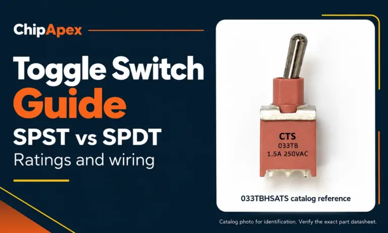
Compare SPST and SPDT toggle switches, understand AC/DC ratings, and follow wiring examples. Check contact action, mounting and parts in the ChipApex catalog.
Read More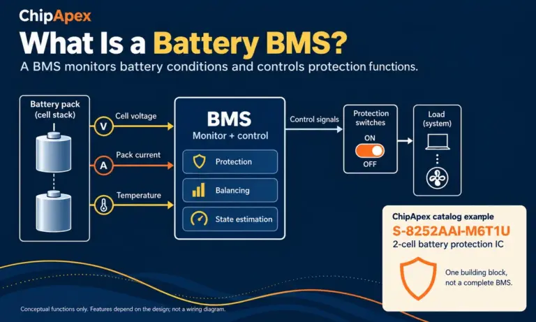
Learn what a battery BMS does, how protection differs from charging, and which pack specifications to check when sourcing BMS components through ChipApex.
Read More
MX25L2026EM1I-12G is listed in the Memory IC range at ChipApex. The manufacturer field lists Macronix. Its product description is IC FLASH 2MBIT SPI 86MHZ…
Read More
MX25L2026EM1I-12G is listed in the Memory IC range at ChipApex. The manufacturer field lists Macronix. Its product description is IC FLASH 2MBIT SPI 86MHZ…
Read More
MX25L2026EM1I-12G is listed in the Memory IC range at ChipApex. The manufacturer field lists Macronix. Its product description is IC FLASH 2MBIT SPI 86MHZ…
Read More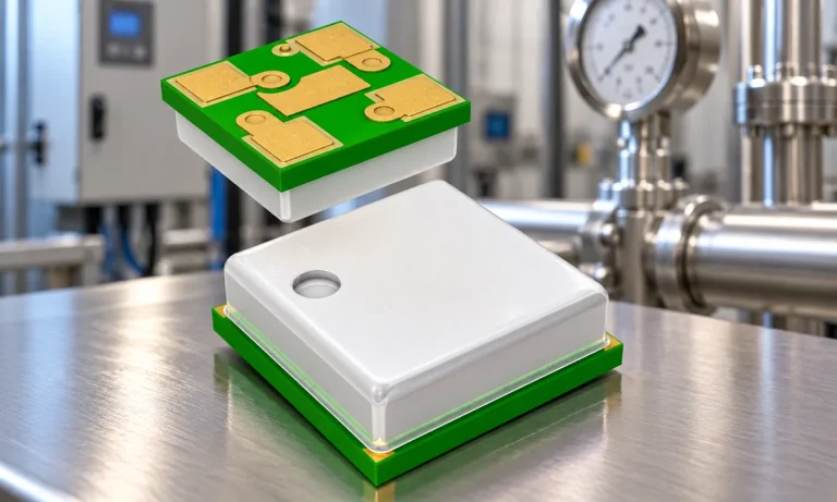
Learn how a pressure transducer converts pressure into voltage, current, or digital output, and compare pressure references and key selection specs.
Read More
The activity of extra discounts on wholesale prices is in full swing…
Please fill in your contact information and we will send you the latest wholesale price list.





